
Datasheet

49
AT32UC3A
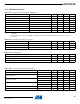
12.8 ADC Characteristics
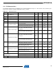
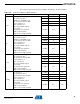
Notes: 1. Corresponds to 13 clock cycles at 5 MHz: 3 clock cycles for track and hold acquisition time and 10 clock cycles for
conversion.
2. Corresponds to 15 clock cycles at 8 MHz: 5 clock cycles for track and hold acquisition time and 10 clock cycles for
conversion.
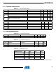
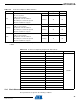
Note: ADVREF should be connected to GND to avoid extra consumption in case ADC is not used.
Table 12-17. Channel Conversion Time and ADC Clock
Parameter Conditions Min Typ Max Units
ADC Clock Frequency 10-bit resolution mode 5 MHz
ADC Clock Frequency 8-bit resolution mode 8 MHz
Startup Time Return from Idle Mode 20 µs
Track and Hold Acquisition Time 600 ns
Conversion Time ADC Clock = 5 MHz 2 µs
Conversion Time ADC Clock = 8 MHz 1.25 µs
Throughput Rate ADC Clock = 5 MHz 384
(1)
kSPS
Throughput Rate ADC Clock = 8 MHz 533
(2)
kSPS
Table 12-18. External Voltage Reference Input
Parameter Conditions Min Typ Max Units
ADVREF Input Voltage Range 2.6 VDDANA V
ADVREF Average Current On 13 samples with ADC Clock = 5 MHz 200 250 µA
Current Consumption on VDDANA 1.25 mA
Table 12-19. Analog Inputs
Parameter Min Typ Max Units
Input Voltage Range 0V
ADVREF
Input Leakage Current 1 µA
Input Capacitance 17 pF
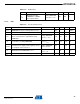
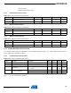
Table 12-20. Transfer Characteristics in 8-bit mode
Parameter Conditions Min Typ Max Units
Resolution 8Bit
Absolute Accuracy
f=5MHz 0.8 LSB
f=8MHz 1.5 LSB
Integral Non-linearity
f=5MHz 0.35 0.5 LSB
f=8MHz 0.5 1.0 LSB
Differential Non-linearity
f=5MHz 0.3 0.5 LSB
f=8MHz 0.5 1.0 LSB
Offset Error f=5MHz -0.5 0.5 LSB
Gain Error f=5MHz -0.5 0.5 LSB
32058KS–AVR32–01/12