
Datasheet


37
32072SH–AVR32–10/2012
AT32UC3A3
5.4 CPU Local Bus Mapping
Some of the registers in the GPIO module are mapped onto the CPU local bus, in addition to
being mapped on the Peripheral Bus. These registers can therefore be reached both by
accesses on the Peripheral Bus, and by accesses on the local bus.
Mapping these registers on the local bus allows cycle-deterministic toggling of GPIO pins since
the CPU and GPIO are the only modules connected to this bus. Also, since the local bus runs at
CPU speed, one write or read operation can be performed per clock cycle to the local bus-
mapped GPIO registers.
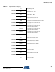
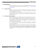
The following GPIO registers are mapped on the local bus:
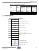
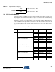
0xFFFF5000
TWIS0 Two-wire Slave Interface - TWIS0
0xFFFF5400
TWIS1 Two-wire Slave Interface - TWIS1
Table 5-2. Peripheral Address Mapping
Table 5-3. Local Bus Mapped GPIO Registers
Port Register Mode
Local Bus
Address Access
0 Output Driver Enable Register (ODER) WRITE 0x40000040 Write-only
SET 0x40000044 Write-only
CLEAR 0x40000048 Write-only
TOGGLE 0x4000004C Write-only
Output Value Register (OVR) WRITE 0x40000050 Write-only
SET 0x40000054 Write-only
CLEAR 0x40000058 Write-only
TOGGLE 0x4000005C Write-only
Pin Value Register (PVR) - 0x40000060 Read-only
1 Output Driver Enable Register (ODER) WRITE 0x40000140 Write-only
SET 0x40000144 Write-only
CLEAR 0x40000148 Write-only
TOGGLE 0x4000014C Write-only
Output Value Register (OVR) WRITE 0x40000150 Write-only
SET 0x40000154 Write-only
CLEAR 0x40000158 Write-only
TOGGLE 0x4000015C Write-only
Pin Value Register (PVR) - 0x40000160 Read-only