Features • High Performance, Low Power 32-bit Atmel® AVR® Microcontroller • • • • • • • • • • • • – Compact Single-Cycle RISC Instruction Set Including DSP Instruction Set – Read-Modify-Write Instructions and Atomic Bit Manipulation – Performing up to 1.
AT32UC3A3 • • • • • • • • • – Support for SPI and LIN – Optionnal support for IrDA, ISO7816, Hardware Handshaking, RS485 interfaces and Modem Line Two Master/Slave Serial Peripheral Interfaces (SPI) with Chip Select Signals One Synchronous Serial Protocol Controller – Supports I2S and Generic Frame-Based Protocols Two Master/Slave Two-Wire Interface (TWI), 400kbit/s I2C-compatible 16-bit Stereo Audio Bitstream – Sample Rate Up to 50 KHz QTouch® Library Support – Capacitive Touch Buttons, Sliders, and W
AT32UC3A3 1. Description The AT32UC3A3/A4 is a complete System-On-Chip microcontroller based on the AVR32 UC RISC processor running at frequencies up to 84MHz. AVR32 UC is a high-performance 32-bit RISC microprocessor core, designed for cost-sensitive embedded applications, with particular emphasis on low power consumption, high code density and high performance.
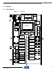
AT32UC3A3 2. Overview Block Diagram NEXUS CLASS 2+ OCD MCKO MDO[5..0] MSEO[1..
AT32UC3A3 2.2 Configuration Summary The table below lists all AT32UC3A3/A4 memory and package configurations: Table 2-1.
AT32UC3A3 3. Package and Pinout 3.1 Package The device pins are multiplexed with peripheral functions as described in the Peripheral Multiplexing on I/O Line section. Figure 3-1.
AT32UC3A3 LQFP144 Pinout 108 107 106 105 104 103 102 101 100 99 98 97 96 95 94 93 92 91 90 89 88 87 86 85 84 83 82 81 80 79 78 77 76 75 74 73 TDI TCK RESET_N TDO TMS VDDIO GNDIO PA15 PA14 PC01 PC00 PX31 PX30 PX33 PX29 PX32 PX25 PX28 PX26 PX27 PX43 PX52 PX24 PX23 PX18 PX17 GNDIO VDDIO PX21 PX55 PX56 PX51 PX57 PX50 PX46 PX20 Figure 3-2.
AT32UC3A3 Figure 3-3.
AT32UC3A3 3.2 Peripheral Multiplexing on I/O lines 3.2.1 Multiplexed Signals Each GPIO line can be assigned to one of the peripheral functions. The following table describes the peripheral signals multiplexed to the GPIO lines. Note that GPIO 44 is physically implemented in silicon but it must be kept unused and configured in input mode. Table 3-1.
AT32UC3A3 Table 3-1.
AT32UC3A3 Table 3-1.
AT32UC3A3 Table 3-1. GPIO Controller Function Multiplexing GPIO function G P BGA QFP BGA 144 144 100 J4 PIN I Type PIN O Supply (2) A B C 78 PX56 107 VDDIO x2 EBI - ADDR[21] EIC - SCAN[2] USART2 - TXD H4 76 PX57 108 VDDIO x2 EBI - ADDR[20] EIC - SCAN[1] USART3 - RXD H3 57 EIC - SCAN[0] USART3 - TXD G3 56 F1(1) PX58 109 VDDIO x2 EBI - NCS[0] PX59 110 VDDIO x2 EBI - NANDWE Note: D MCI - CMD[1] 1. Those balls are physically connected to 2 GPIOs.
AT32UC3A3 3.2.4 JTAG port connections Table 3-4. 3.2.5 JTAG Pinout TFBGA144 QFP144 VFBGA100 Pin name JTAG pin K12 107 K9 TCK TCK L12 108 K8 TDI TDI J11 105 J8 TDO TDO J10 104 H7 TMS TMS Nexus OCD AUX port connections If the OCD trace system is enabled, the trace system will take control over a number of pins, irrespective of the GPIO configuration. Three differents OCD trace pin mappings are possible, depending on the configuration of the OCD AXS register.
AT32UC3A3 3.3 Signal Descriptions The following table gives details on signal name classified by peripheral. Table 3-6. Signal Description List Signal Name Function Type Active Level Comments Power VDDIO I/O Power Supply Power 3.0 to 3.6V VDDANA Analog Power Supply Power 3.0 to 3.6V VDDIN Voltage Regulator Input Supply Power 3.0 to 3.6V VDDCORE Voltage Regulator Output for Digital Supply Power Output 1.65 to 1.
AT32UC3A3 Table 3-6.
AT32UC3A3 Table 3-6.
AT32UC3A3 Table 3-6.
AT32UC3A3 Table 3-6. Signal Description List Signal Name Function Type DMHS USB High Speed Data - Analog DPHS USB High Speed Data + Analog USB_VBIAS USB VBIAS reference Analog USB_VBUS USB VBUS signal Output VBOF USB VBUS on/off bus power control port Output ID ID Pin fo the USB bus Active Level Comments Connect to the ground through a 6810 ohms (+/- 1%) resistor in parallel with a 10pf capacitor.
AT32UC3A3 3.4 3.4.1 I/O Line Considerations JTAG Pins TMS and TDI pins have pull-up resistors. TDO pin is an output, driven at up to VDDIO, and has no pull-up resistor. 3.4.2 RESET_N Pin The RESET_N pin is a schmitt input and integrates a permanent pull-up resistor to VDDIO. As the product integrates a power-on reset cell, the RESET_N pin can be left unconnected in case no reset from the system needs to be applied to the product. 3.4.
AT32UC3A3 3.5 3.5.1 Power Considerations Power Supplies The AT32UC3A3 has several types of power supply pins: • • • • VDDIO: Powers I/O lines. Voltage is 3.3V nominal VDDANA: Powers the ADC. Voltage is 3.3V nominal VDDIN: Input voltage for the voltage regulator. Voltage is 3.3V nominal VDDCORE: Output voltage from regulator for filtering purpose and provides the supply to the core, memories, and peripherals. Voltage is 1.8V nominal The ground pin GNDCORE is common to VDDCORE and VDDIN.
AT32UC3A3 4. Processor and Architecture Rev: 1.4.2.0 This chapter gives an overview of the AVR32UC CPU. AVR32UC is an implementation of the AVR32 architecture. A summary of the programming model, instruction set, and MPU is presented. For further details, see the AVR32 Architecture Manual and the AVR32UC Technical Reference Manual. 4.
AT32UC3A3 The register file is organized as sixteen 32-bit registers and includes the Program Counter, the Link Register, and the Stack Pointer. In addition, register R12 is designed to hold return values from function calls and is used implicitly by some instructions. 4.3 The AVR32UC CPU The AVR32UC CPU targets low- and medium-performance applications, and provides an advanced OCD system, no caches, and a Memory Protection Unit (MPU). Java acceleration hardware is not implemented.
AT32UC3A3 OCD interface Reset interface Overview of the AVR32UC CPU Interrupt controller interface Figure 4-1. OCD system Power/ Reset control AVR32UC CPU pipeline MPU 4.3.
AT32UC3A3 Figure 4-2. The AVR32UC Pipeline Multiply unit MUL IF ID Pref etch unit Decode unit Regf ile Read A LU LS 4.3.2 Regf ile w rite A LU unit Load-store unit AVR32A Microarchitecture Compliance AVR32UC implements an AVR32A microarchitecture. The AVR32A microarchitecture is targeted at cost-sensitive, lower-end applications like smaller microcontrollers. This microarchitecture does not provide dedicated hardware registers for shadowing of register file registers in interrupt contexts.
AT32UC3A3 The following table shows the instructions with support for unaligned addresses. All other instructions require aligned addresses. Table 4-1. 4.3.6 Instructions with Unaligned Reference Support Instruction Supported alignment ld.d Word st.
AT32UC3A3 4.4 4.4.1 Programming Model Register File Configuration The AVR32UC register file is shown below. Figure 4-3.
AT32UC3A3 Figure 4-5. The Status Register Low Halfword Bit 15 Bit 0 - T - - - - - - - - L Q V N Z C Bit name 0 0 0 0 0 0 0 0 0 0 0 0 0 0 0 0 Initial value Carry Zero Sign Overflow Saturation Lock Reserved Scratch Reserved 4.4.3 4.4.3.1 Processor States Normal RISC State The AVR32 processor supports several different execution contexts as shown in Table 4-2 on page 27. Table 4-2. Overview of Execution Modes, their Priorities and Privilege Levels.
AT32UC3A3 All interrupt levels are by default disabled when debug state is entered, but they can individually be switched on by the monitor routine by clearing the respective mask bit in the status register. Debug state can be entered as described in the AVR32UC Technical Reference Manual. Debug state is exited by the retd instruction. 4.4.4 System Registers The system registers are placed outside of the virtual memory space, and are only accessible using the privileged mfsr and mtsr instructions.
AT32UC3A3 Table 4-3.
AT32UC3A3 Table 4-3. 4.
AT32UC3A3 The user must also make sure that the system stack is large enough so that any event is able to push the required registers to stack. If the system stack is full, and an event occurs, the system will enter an UNDEFINED state. 4.5.2 Exceptions and Interrupt Requests When an event other than scall or debug request is received by the core, the following actions are performed atomically: 1. The pending event will not be accepted if it is masked.
AT32UC3A3 status register. Upon entry into Debug mode, hardware sets the SR[D] bit and jumps to the Debug Exception handler. By default, Debug mode executes in the exception context, but with dedicated Return Address Register and Return Status Register. These dedicated registers remove the need for storing this data to the system stack, thereby improving debuggability.
AT32UC3A3 Table 4-4.
AT32UC3A3 5. Memories 5.
AT32UC3A3 Table 5-1. 5.3 AT32UC3A3A4 Physical Memory Map Size Size Size Device Start Address AT32UC3A3256S AT32UC3A3256 AT32UC3A4256S AT32UC3A4256 AT32UC3A3128S AT32UC3A3128 AT32UC3A4128S AT32UC3A4128 AT32UC3A364S AT32UC3A364 AT32UC3A464S AT32UC3A464 HRAMC0 0xFF000000 32KByte 32KByte 32KByte HRAMC1 0xFF008000 32KByte 32KByte 32KByte HSB-PB Bridge A 0xFFFF0000 64KByte 64KByte 64KByte HSB-PB Bridge B 0xFFFE0000 64KByte 64KByte 64KByte Peripheral Address Map Table 5-2.
AT32UC3A3 Table 5-2.
AT32UC3A3 Table 5-2. Peripheral Address Mapping 0xFFFF5000 TWIS0 Two-wire Slave Interface - TWIS0 TWIS1 Two-wire Slave Interface - TWIS1 0xFFFF5400 5.4 CPU Local Bus Mapping Some of the registers in the GPIO module are mapped onto the CPU local bus, in addition to being mapped on the Peripheral Bus. These registers can therefore be reached both by accesses on the Peripheral Bus, and by accesses on the local bus.
AT32UC3A3 Table 5-3.
AT32UC3A3 6. Boot Sequence This chapter summarizes the boot sequence of the AT32UC3A3/A4. The behavior after powerup is controlled by the Power Manager. For specific details, refer to Section 7. ”Power Manager (PM)” on page 86. 6.1 Starting of Clocks After power-up, the device will be held in a reset state by the Power-On Reset circuitry, until the power has stabilized throughout the device. Once the power has stabilized, the device will use the internal RC Oscillator as clock source.
AT32UC3A3 7. Electrical Characteristics 7.1 Absolute Maximum Ratings* Operating Temperature.................................... -40°C to +85°C Storage Temperature ..................................... -60°C to +150°C Voltage on Input Pin with respect to Ground ........................................-0.3V to 3.6V Maximum Operating Voltage (VDDCORE) ..................... 1.95V *NOTICE: Stresses beyond those listed under “Absolute Maximum Ratings” may cause permanent damage to the device.
AT32UC3A3 7.2 DC Characteristics The following characteristics are applicable to the operating temperature range: T A = -40°C to 85°C, unless otherwise specified and are certified for a junction temperature up toTJ = 100°C. Table 7-1. DC Characteristics Symbol Parameter VVDDIO DC Supply Peripheral I/Os VVDDANA DC Analog Supply Conditions Min. Max. Unit 3.0 3.6 V 3.0 3.6 V -0.3 +0.8 V TWCK, TWD VVDDIO x0.7 VVDDIO +0.5 V RESET_N, TCK, TDI +0.
AT32UC3A3 7.2.1 I/O Pin Output Level Typical Characteristics Figure 7-1. I/O Pin drive x2 Output Low Level Voltage (VOL) vs. Source Current VddIo = 3.3V 1,8 90 1,6 25 1,4 -45 Voltage [V 1,2 1 0,8 0,6 0,4 0,2 0 0 5 10 15 20 Load current [mA] Figure 7-2. I/O Pin drive x2 Output High Level Voltage (VOH) vs. Source Current VddIo = 3.3V 3,5 3 Voltage [V 2,5 -45 25 90 2 1,5 1 0,5 0 0 5 10 15 20 Load current [mA] 7.
AT32UC3A3 Table 7-2. Symbol fMAX Parameter Output frequency Rise time tRISE Fall time tFALL 7.4 Normal I/O Pin Characteristics Conditions drive x2 drive x2 drive x3 Unit 10pf 40 66 100 MHz 30pf 18.2 35.7 61.6 MHz 60pf 7.5 18.5 36.3 MHz 10pf 2.7 1.4 0.9 ns 30pf 6.9 3.5 1.9 ns 60pf 13.4 6.7 3.5 ns 10pf 3.2 1.7 0.9 ns 30pf 8.6 4.3 2.26 ns 60pf 16.5 8.3 4.3 ns Regulator characteristics Table 7-3.
AT32UC3A3 7.5 Analog characteristics 7.5.1 ADC Table 7-5. Electrical Characteristics Symbol Parameter VVDDANA Analog Power Supply Table 7-6. Conditions Typ. Max. Unit 3.0 3.6 V Typ. Technology Unit 100 NPO nF Decoupling Requirements Symbol Parameter CVDDANA Power Supply Capacitor 7.5.2 Min. Conditions BOD Table 7-7. Symbol 1.8V BOD Level Values Parameter Value Conditions Min. Typ. Max. Unit 00 1111b 1.79 V 01 0111b 1.70 V 01 1111b 1.61 V 10 0111b 1.
AT32UC3A3 Table 7-9. BOD Timing Symbol Parameter Conditions TBOD Minimum time with VDDCORE < VBOD to detect power failure Falling VDDCORE from 1.8V to 1.1V 7.5.3 Min. Typ. Max. Unit 300 800 ns Typ. Max. Unit Reset Sequence Table 7-10. Electrical Characteristics Symbol Parameter Conditions Min.
AT32UC3A3 Figure 7-3. VDDIN VDDIO MCU Cold Start-Up VBOD33LEVEL VBOD33LEVEL VRESTART RESET_N Internal BOD33 Reset TSSU1 Internal MCU Reset Figure 7-4. VDDIN VDDIO MCU Cold Start-Up RESET_N Externally Driven VBOD33LEVEL VBOD33LEVEL VRESTART RESET_N Internal BOD33 Reset TSSU1 Internal MCU Reset Figure 7-5.
AT32UC3A3 7.5.4 RESET_N Characteristics Table 7-11. RESET_N Waveform Parameters Symbol Parameter tRESET RESET_N minimum pulse width Conditions Min. 10 Typ. Max.
AT32UC3A3 7.6 Power Consumption The values in Table 7-12 and Table 7-13 on page 50 are measured values of power consumption with operating conditions as follows: •VDDIO = 3.3V •TA = 25°C •I/Os are configured in input, pull-up enabled. Figure 7-6.
AT32UC3A3 Power Consumtion for Different Sleep Modes 7.6.1 Table 7-12. Power Consumption for Different Sleep Modes Conditions(1) Mode Typ. Unit - CPU running a recursive Fibonacci Algorithm from flash and clocked from PLL0 at f MHz. - Flash High Speed mode disable (f < 66 MHz) - Voltage regulator is on. - XIN0: external clock. Xin1 Stopped. XIN32 stopped. - All peripheral clocks activated with a division by 8.
AT32UC3A3 Table 7-13. Peripheral Typical Cuurent Consumption by Peripheral Typ. ADC 7 AES 80 ABDAC 10 DMACA 70 EBI 23 EIC 0.
AT32UC3A3 7.7 System Clock Characteristics These parameters are given in the following conditions: • VDDCORE = 1.8V 7.7.1 CPU/HSB Clock Characteristics Table 7-14. Core Clock Waveform Parameters Symbol Parameter Conditions 1/(tCPCPU) CPU Clock Frequency 1/(tCPCPU) CPU Clock Frequency 7.7.2 Min. Typ. Max. Unit -40°C < Ambient Temperature < 70°C 84 MHz -40°C < Ambient Temperature < 85°C 66 MHz Max. Unit PBA Clock Characteristics Table 7-15.
AT32UC3A3 7.8 Oscillator Characteristics The following characteristics are applicable to the operating temperature range: TA = -40°C to 85°C and worst case of power supply, unless otherwise specified. 7.8.1 Slow Clock RC Oscillator Table 7-17. Symbol RC Oscillator Frequency Parameter Conditions Min. Calibration point: TA = 85°C FRC RC Oscillator Frequency 7.8.2 TA = 25°C Typ. Max. Unit 115.2 116 KHz 112 KHz KHz TA = -40°C 105 108 Conditions Min. Typ. 32 KHz Oscillator Table 7-18.
AT32UC3A3 7.8.3 Main Oscillators Table 7-19. Main Oscillators Characteristics Symbol Parameter 1/(tCPMAIN) Oscillator Frequency CL1, CL2 Internal Load Capacitance (CL1 = CL2) ESR Crystal Equivalent Series Resistance Conditions Min. Typ. External clock on XIN Crystal 0.4 Max. Unit 50 MHz 20 MHz 7 Duty Cycle 40 f = 400 KHz f = 8 MHz f = 16 MHz f = 20 MHz 50 pF 75 Ω 60 % 25 4 1.4 1 tST Startup Time tCH XIN Clock High Half-period 0.4 tCP 0.
AT32UC3A3 7.9 ADC Characteristics Table 7-22. Channel Conversion Time and ADC Clock Parameter Conditions ADC Clock Frequency Startup Time Max. Unit 10-bit resolution mode 5 MHz 8-bit resolution mode 8 MHz Return from Idle Mode 20 µs Track and Hold Acquisition Time Min. Typ. 600 ns ADC Clock = 5 MHz Conversion Time Throughput Rate 2 µs ADC Clock = 8 MHz 1.25 µs ADC Clock = 5 MHz 384 (1) kSPS ADC Clock = 8 MHz 533 (2) kSPS 1.
AT32UC3A3 Table 7-26. Transfer Characteristics in 10-bit mode Parameter Conditions Min. Typ. Resolution Max. Unit 3 LSB 10 Bit Absolute Accuracy ADC Clock = 5 MHz Integral Non-linearity ADC Clock = 5 MHz 1.5 2 LSB ADC Clock = 5 MHz 1 2 LSB 0.6 1 LSB Differential Non-linearity ADC Clock = 2.5 MHz Offset Error ADC Clock = 5 MHz -2 2 LSB Gain Error ADC Clock = 5 MHz -2 2 LSB Max. Unit 7.10 USB Transceiver Characteristics 7.10.1 Electrical Characteristics Table 7-27.
AT32UC3A3 Table 7-29. Symbol IVDDUTMI 1. 34.5.5 Dynamic Power Consumption Parameter Conditions HS Transceiver current consumption Min. Typ. Max. Unit HS transmission 47 60 mA HS Transceiver current consumption HS reception 18 27 mA FS/HS Transceiver current consumption FS transmission 0m cable (1) 4 6 mA FS/HS Transceiver current consumption FS transmission 5m cable 26 30 mA FS/HS Transceiver current consumption FS reception 3 4.
AT32UC3A3 7.11 EBI Timings 7.11.1 SMC Signals These timings are given for worst case process, T = 85⋅C, VDDIO = 3V and 40 pF load capacitance. Table 7-30. SMC Clock Signal Symbol Parameter Max.(1) Unit 1/(tCPSMC) SMC Controller Clock Frequency 1/(tcpcpu) MHz Note: 1. The maximum frequency of the SMC interface is the same as the max frequency for the HSB. Table 7-31. Symbol SMC Read Signals with Hold Settings Parameter Min.
AT32UC3A3 Table 7-32. Symbol SMC Read Signals with no Hold Settings Parameter Min. Unit 13.7 ns 1 ns 13.3 ns 0 ns Min. Unit NRD Controlled (READ_MODE = 1) SMC19 Data Setup before NRD High SMC20 Data Hold after NRD High NRD Controlled (READ_MODE = 0) SMC21 Data Setup before NCS High SMC22 Data Hold after NCS High Table 7-33. Symbol SMC Write Signals with Hold Settings Parameter NRD Controlled (READ_MODE = 1) SMC23 Data Out Valid before NWE High (nwe pulse length - 1) * tCPSMC - 0.
AT32UC3A3 Table 7-34. SMC Write Signals with No Hold Settings (NWE Controlled only) Symbol Parameter SMC43 Data Out Valid before NWE Rising SMC44 Data Out Valid after NWE Rising SMC45 NWE Pulse Width Figure 7-7. Min. Unit (nwe pulse length - 1) * tCPSMC - 1.2 ns 5 ns nwe pulse length * tCPSMC - 0.9 ns SMC Signals for NCS Controlled Accesses.
AT32UC3A3 Figure 7-8. SMC Signals for NRD and NRW Controlled Accesses. SMC37 SMC7 SMC7 SMC31 A2-A25 SMC25 SMC26 SMC29 SMC30 SMC3 SMC4 SMC5 SMC6 SMC38 SMC39 SMC40 SMC41 SMC3 SMC4 SMC5 SMC6 A0/A1/NBS[3:0] SMC42 SMC32 SMC8 NCS SMC8 SMC9 SMC9 NRD SMC19 SMC20 SMC43 SMC44 SMC1 SMC23 SMC2 SMC24 D0 - D15 SMC33 SMC45 NWE 7.11.2 SDRAM Signals These timings are given for 10 pF load on SDCK and 40 pF on other signals. Table 7-35. SDRAM Clock Signal.
AT32UC3A3 Table 7-36. SDRAM Clock Signal Symbol Parameter Conditions Min. Max. Unit SDRAMC13 Bank Change before SDCK Rising Edge 6.3 ns SDRAMC14 Bank Change after SDCK Rising Edge 2.4 ns SDRAMC15 CAS Low before SDCK Rising Edge 7.4 ns SDRAMC16 CAS High after SDCK Rising Edge 1.9 ns SDRAMC17 DQM Change before SDCK Rising Edge 6.4 ns SDRAMC18 DQM Change after SDCK Rising Edge 2.
AT32UC3A3 Figure 7-9. SDRAMC Signals relative to SDCK.
AT32UC3A3 7.12 JTAG Characteristics 7.12.1 JTAG Interface Signals Table 7-37. JTAG Interface Timing Specification Conditions (1) Symbol Parameter Min. Max.
AT32UC3A3 Figure 7-10. JTAG Interface Signals JTAG2 TCK JTAG JTAG1 0 TMS/TDI JTAG3 JTAG4 JTAG7 JTAG8 TDO JTAG5 JTAG6 Device Inputs Device Outputs JTAG9 JTAG10 7.13 SPI Characteristics Figure 7-11.
AT32UC3A3 Figure 7-12. SPI Master mode with (CPOL= 0 and NCPHA= 1) or (CPOL= 1 and NCPHA= 0) SPCK SPI3 SPI4 MISO SPI5 MOSI Figure 7-13. SPI Slave mode with (CPOL= 0 and NCPHA= 1) or (CPOL= 1 and NCPHA= 0) SPCK SPI6 MISO SPI7 SPI8 MOSI Figure 7-14.
AT32UC3A3 Table 7-38. SPI Timings Symbol Parameter Conditions (1) SPI0 MISO Setup time before SPCK rises (master) 3.3V domain 22 + (tCPMCK)/2 (2) ns SPI1 MISO Hold time after SPCK rises (master) 3.3V domain 0 ns SPI2 SPCK rising to MOSI Delay (master) 3.3V domain SPI3 MISO Setup time before SPCK falls (master) 3.3V domain 22 + (tCPMCK)/2 (3) ns SPI4 MISO Hold time after SPCK falls (master) 3.3V domain 0 ns SPI5 SPCK falling to MOSI Delay master) 3.
AT32UC3A3 7.15 Flash Memory Characteristics The following table gives the device maximum operating frequency depending on the field FWS of the Flash FSR register. This field defines the number of wait states required to access the Flash Memory. Flash operating frequency equals the CPU/HSB frequency. Table 7-39. Symbol FFOP Table 7-40. Flash Operating Frequency Parameter Conditions Min. Typ. Max.
AT32UC3A3 8. Mechanical Characteristics 8.1 8.1.1 Thermal Considerations Thermal Data Table 8-1 summarizes the thermal resistance data depending on the package. Table 8-1. 8.1.2 Thermal Resistance Data Symbol Parameter Condition Package Typ θJA Junction-to-ambient thermal resistance Still Air TQFP144 40.3 θJC Junction-to-case thermal resistance TQFP144 9.5 θJA Junction-to-ambient thermal resistance TFBGA144 28.5 θJC Junction-to-case thermal resistance TFBGA144 6.
AT32UC3A3 8.2 Package Drawings Figure 8-1.
AT32UC3A3 Figure 8-2. LQFP-144 package drawing Table 8-2. Device and Package Maximum Weight 1300 Table 8-3. mg Package Characteristics Moisture Sensitivity Level Table 8-4.
AT32UC3A3 Figure 8-3.
AT32UC3A3 8.3 Soldering Profile Table 8-5 gives the recommended soldering profile from J-STD-20. Table 8-5. Soldering Profile Profile Feature Green Package Average Ramp-up Rate (217°C to Peak) 3°C/Second max Preheat Temperature 175°C ±25°C 150-200°C Time Maintained Above 217°C 60-150 seconds Time within 5°C of Actual Peak Temperature 30 seconds Peak Temperature Range 260 (+0/-5°C) Ramp-down Rate 6°C/Second max.
AT32UC3A3 9.
AT32UC3A3 10. Errata 10.1 10.1.1 Rev. H General Devices with Date Code lower than 1233 cannot operate with CPU frequency higher than 66MHz in 1WS and 36MHz in 0WS in the whole temperature range Fix/Workaround None DMACA data transfer fails when CTLx.SRC_TR_WIDTH is not equal CTLx.DST_TR_WIDTH Fix/Workaround For any DMACA transfer make sure CTLx.SRC_TR_WIDTH = CTLx.DST_TR_WIDTH. 10.1.
AT32UC3A3 For higher polling time, the software must freeze the pipe for the desired period in order to prevent any "extra" token. 10.1.5 ADC Sleep Mode activation needs additional A to D conversion If the ADC sleep mode is activated when the ADC is idle the ADC will not enter sleep mode before after the next AD conversion. Fix/Workaround Activate the sleep mode in the mode register and then perform an AD conversion. 10.1.
AT32UC3A3 SPI data transfer hangs with CSR0.CSAAT==1 and MR.MODFDIS==0 When CSR0.CSAAT==1 and mode fault detection is enabled (MR.MODFDIS==0), the SPI module will not start a data transfer. Fix/Workaround Disable mode fault detection by writing a one to MR.MODFDIS. Disabling SPI has no effect on the SR.TDRE bit Disabling SPI has no effect on the SR.TDRE bit whereas the write data command is filtered when SPI is disabled. Writing to TDR when SPI is disabled will not clear SR.TDRE.
AT32UC3A3 10.1.10 AES URAD (Unspecified Register Access Detection Status) does not detect read accesses to the write-only KEYW[5..8]R registers Fix/Workaround None. 10.1.11 HMATRIX In the PRAS and PRBS registers, the MxPR fields are only two bits In the PRAS and PRBS registers, the MxPR fields are only two bits wide, instead of four bits. The unused bits are undefined when reading the registers. Fix/Workaround Mask undefined bits when reading PRAS and PRBS. 10.1.12 TWIM TWIM SR.
AT32UC3A3 TWIS stretch on Address match error When the TWIS stretches TWCK due to a slave address match, it also holds TWD low for the same duration if it is to be receiving data. When TWIS releases TWCK, it releases TWD at the same time. This can cause a TWI timing violation. Fix/Workaround None. 10.1.
AT32UC3A3 Fix/Workaround Set to 1b bit CORRS4 of the ECCHRS mode register (MD). In C-code: *((volatile int*) (0xFFFE2404))= 0x400. DMACA data transfer fails when CTLx.SRC_TR_WIDTH is not equal CTLx.DST_TR_WIDTH Fix/Workaround For any DMACA transfer make sure CTLx.SRC_TR_WIDTH = CTLx.DST_TR_WIDTH. to 3.3V supply monitor is not available FGPFRLO[30:29] are reserved and should not be used by the application. Fix/Workaround None. Service access bus (SAB) can not access DMACA registers Fix/Workaround None. 10.
AT32UC3A3 Fix/Workaround For higher polling time, the software must freeze the pipe for the desired period in order to prevent any "extra" token. 10.2.5 ADC Sleep Mode activation needs additional A to D conversion If the ADC sleep mode is activated when the ADC is idle the ADC will not enter sleep mode before after the next AD conversion. Fix/Workaround Activate the sleep mode in the mode register and then perform an AD conversion. 10.2.
AT32UC3A3 Fix/Workaround SOFT_RESET on RX+ Config US_MR + Config_US_CR. 10.2.7 SPI SPI disable does not work in SLAVE mode SPI disable does not work in SLAVE mode. Fix/Workaround Read the last received data, then perform a software reset by writing a one to the Software Reset bit in the Control Register (CR.SWRST). SPI bad serial clock generation on 2nd chip_select when SCBR=1, CPOL=1, and NCPHA=0 When multiple chip selects (CS) are in use, if one of the baudrates equal 1 while one (CSRn.
AT32UC3A3 Fix/Workaround Before going to sleep modes where the system RC oscillator is stopped, make sure that the factor between the CPU/HSB and PBx frequencies is less than or equal to 4. 10.2.9 PDCA PCONTROL.CHxRES is non-functional PCONTROL.CHxRES is non-functional. Counters are reset at power-on, and cannot be reset by software. Fix/Workaround Software needs to keep history of performance counters.
AT32UC3A3 SMBALERT bit may be set after reset The SMBus Alert (SMBALERT) bit in the Status Register (SR) might be erroneously set after system reset. Fix/Workaround After system reset, clear the SR.SMBALERT bit before commencing any TWI transfer. 10.2.
AT32UC3A3 10.2.16 FLASHC Corrupted read in flash may happen after fuses write or erase operations (FLASHC LP, UP, WGPB, EGPB, SSB, PGPFB, EAGPF commands) After a flash fuse write or erase operation (FLASHC LP, UP, WGPB, EGPB, SSB, PGPFB, EAGPF commands), reading (data read or code fetch) in flash may fail. This may lead to an exception or to other errors derived from this corrupted read access.
AT32UC3A3 When the main clock is RCSYS, TIMER_CLOCK5 is equal to PBA clock When the main clock is generated from RCSYS, TIMER_CLOCK5 is equal to PBA Clock and not PBA Clock / 128. Fix/Workaround None. RETE instruction does not clear SREG[L] from interrupts The RETE instruction clears SREG[L] as expected from exceptions. Fix/Workaround When using the STCOND instruction, clear SREG[L] in the stacked value of SR before returning from interrupts with RETE.
AT32UC3A3 10.3.5 ADC Sleep Mode activation needs additional A to D conversion If the ADC sleep mode is activated when the ADC is idle the ADC will not enter sleep mode before after the next AD conversion. Fix/Workaround Activate the sleep mode in the mode register and then perform an AD conversion. 10.3.6 USART ISO7816 info register US_NER cannot be read The NER register always returns zero. Fix/Workaround None.
AT32UC3A3 10.3.7 SPI SPI disable does not work in SLAVE mode SPI disable does not work in SLAVE mode. Fix/Workaround Read the last received data, then perform a software reset by writing a one to the Software Reset bit in the Control Register (CR.SWRST). SPI bad serial clock generation on 2nd chip_select when SCBR=1, CPOL=1, and NCPHA=0 When multiple chip selects (CS) are in use, if one of the baudrates equal 1 while one (CSRn.SCBR=1) of the others do not equal 1, and CSRn.CPOL=1 and CSRn.
AT32UC3A3 10.3.9 PDCA PCONTROL.CHxRES is non-functional PCONTROL.CHxRES is non-functional. Counters are reset at power-on, and cannot be reset by software. Fix/Workaround Software needs to keep history of performance counters.
AT32UC3A3 Fix/Workaround None. 10.3.14 MCI The busy signal of the responses R1b is not taken in account for CMD12 STOP_TRANSFER It is not possible to know the busy status of the card during the response (R1b) for the commands CMD12. Fix/Workaround The card busy line should be polled through the GPIO Input Value register (IVR) for commands CMD12. 10.3.
AT32UC3A3 11. Datasheet Revision History Please note that the referring page numbers in this section are referred to this document. The referring revision in this section are referring to the document revision. 11.1 11.2 11.3 11.4 11.5 11.6 Rev. H– 10/12 1. Updated max frequency 2. Added Flash Read High Speed Mode description in FLASHC chapter 3. Updated Electrical Characteristics accordingly to new max frequency 4. Fixed wrong description of PLLOPT[0] in PM chapter 5.
AT32UC3A3 11.7 11.8 Rev. B – 08/09 1. Updated the datasheet with new device AT32UC3A4. 1. Initial revision. Rev.
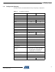
AT32UC3A3 1 Description ............................................................................................... 3 2 Overview ................................................................................................... 4 3 4 5 6 7 2.1 Block Diagram ...................................................................................................4 2.2 Configuration Summary .....................................................................................5 Package and Pinout ...
AT32UC3A3 8 9 7.10 USB Transceiver Characteristics .....................................................................55 7.11 EBI Timings .....................................................................................................57 7.12 JTAG Characteristics .......................................................................................63 7.13 SPI Characteristics ..........................................................................................64 7.14 MCI .............
Atmel Corporation 2325 Orchard Parkway San Jose, CA 95131 USA Tel: (+1)(408) 441-0311 Fax: (+1)(408) 487-2600 www.atmel.com Atmel Asia Limited Unit 1-5 & 16, 19/F BEA Tower, Millennium City 5 418 Kwun Tong Road Kwun Tong, Kowloon HONG KONG Tel: (+852) 2245-6100 Fax: (+852) 2722-1369 Atmel Munich GmbH Business Campus Parkring 4 D-85748 Garching b. Munich GERMANY Tel: (+49) 89-31970-0 Fax: (+49) 89-3194621 Atmel Japan 16F, Shin Osaki Kangyo Bldg.