
Datasheet


22
32072SH–AVR32–10/2012
AT32UC3A3
The register file is organized as sixteen 32-bit registers and includes the Program Counter, the
Link Register, and the Stack Pointer. In addition, register R12 is designed to hold return values
from function calls and is used implicitly by some instructions.
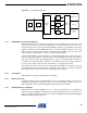
4.3 The AVR32UC CPU
The AVR32UC CPU targets low- and medium-performance applications, and provides an
advanced OCD system, no caches, and a Memory Protection Unit (MPU). Java acceleration
hardware is not implemented.
AVR32UC provides three memory interfaces, one High Speed Bus master for instruction fetch,
one High Speed Bus master for data access, and one High Speed Bus slave interface allowing
other bus masters to access data RAMs internal to the CPU. Keeping data RAMs internal to the
CPU allows fast access to the RAMs, reduces latency, and guarantees deterministic timing.
Also, power consumption is reduced by not needing a full High Speed Bus access for memory
accesses. A dedicated data RAM interface is provided for communicating with the internal data
RAMs.
A local bus interface is provided for connecting the CPU to device-specific high-speed systems,
such as floating-point units and fast GPIO ports. This local bus has to be enabled by writing the
LOCEN bit in the CPUCR system register. The local bus is able to transfer data between the
CPU and the local bus slave in a single clock cycle. The local bus has a dedicated memory
range allocated to it, and data transfers are performed using regular load and store instructions.
Details on which devices that are mapped into the local bus space is given in the Memories
chapter of this data sheet.
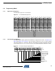
Figure 4-1 on page 23 displays the contents of AVR32UC.