
User Manual


CONFIDENTIAL
© 2000~2011 iSSC Technologies Corp.
8
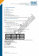
- Timing Sequence
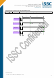
Timing Sequence for Mode selection Pin (P20, P24) under APP mode
Pin No. I/O Name Description
4 I BAT_IN 3.3V power input
7 P VDD_IO
Main power supply
17 I P20
System configuration, refer to P2_4, MCU do NOT drive under APP Mode
18 I P24
Boot mode selection (MCU NOT drive under APP Mode)
P2_0/ P2_4: HH Æ Application
LL Æ Boot mode
LH Æ HCI UART mode for testing and system configuration.
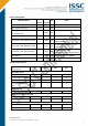
P20
P24
VDDIO
Power
7.28ms 41.1ms
P20, P24 Mode Selection Timing Diagram