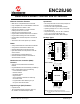
ENC28J60 Stand-Alone Ethernet Controller with SPI Interface Ethernet Controller Features Operational • • • • • • • • • • 28-Pin SPDIP, SSOP, SOIC 8-Kbyte Transmit/Receive Packet Dual Port SRAM Configurable Transmit/Receive Buffer Size Hardware Managed Circular Receive FIFO Byte-Wide Random and Sequential Access with Auto-Increment • Internal DMA for Fast Data Movement • Hardware Assisted Checksum Calculation for Various Network Protocols Medium Access Controller (MAC) Features 28-Pin QFN(2) • Suppor
ENC28J60 Table of Contents 1.0 Overview ...................................................................................................................................................................................... 3 2.0 External Connections ................................................................................................................................................................... 5 3.0 Memory Organization ........................................................................
ENC28J60 1.0 OVERVIEW The ENC28J60 consists of seven major functional blocks: The ENC28J60 is a stand-alone Ethernet controller with an industry standard Serial Peripheral Interface (SPI). It is designed to serve as an Ethernet network interface for any controller equipped with SPI. 1. 2. The ENC28J60 meets all of the IEEE 802.3 specifications. It incorporates a number of packet filtering schemes to limit incoming packets.
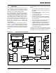
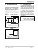
ENC28J60 FIGURE 1-2: TYPICAL ENC28J60 BASED INTERFACE MCU ENC28J60 TPIN+/- CS I/O TPOUT+/- SI SDO SO SDI SCK SCK TX/RX Buffer MAC ETHERNET TRANSFORMER PHY LEDA INT INTX RJ45 LEDB TABLE 1-1: PINOUT I/O DESCRIPTIONS Pin Number SPDIP, SOIC, SSOP QFN Pin Type Buffer Type VCAP 1 25 P — 2.5V output from internal regulator. A low Equivalent Series Resistance (ESR) capacitor, with a typical value of 10 µF and a minimum value of 1 µF to ground, must be placed on this pin.
ENC28J60 2.0 EXTERNAL CONNECTIONS 2.1 Oscillator 2.2 The ENC28J60 contains an Oscillator Start-up Timer (OST) to ensure that the oscillator and integrated PHY have stabilized before use. The OST does not expire until 7500 OSC1 clock cycles (300 s) pass after Power-on Reset or wake-up from Power-Down mode occurs. During the delay, all Ethernet registers and buffer memory may still be read and written to through the SPI bus. However, software should not attempt to transmit any packets (set ECON1.
ENC28J60 2.3 CLKOUT Pin value). Additionally, Power-Down mode may be entered and the CLKOUT function will continue to operate. When Power-Down mode is cancelled, the OST will be reset but the CLKOUT function will continue. When the CLKOUT function is disabled (ECOCON = 0), the CLKOUT pin is driven low. The Clock Out (CLKOUT) pin is provided to the system designer for use as the host controller clock or as a clock source for other devices in the system.
ENC28J60 2.4 Magnetics, Termination and Other External Components A common-mode choke on the TPOUT interface, placed between the TPOUT pins and the Ethernet transformer (not shown), is not recommended. If a common-mode choke is used to reduce EMI emissions, it should be placed between the Ethernet transformer and pins 1 and 2 of the RJ-45 connector. Many Ethernet transformer modules include common-mode chokes inside the same device package.
ENC28J60 2.5 I/O Levels 2.6 The ENC28J60 is a 3.3V part; however, it was designed to be easily integrated into 5V systems. The SPI CS, SCK and SI inputs, as well as the RESET pin, are all 5V tolerant. On the other hand, if the host controller is operated at 5V, it quite likely will not be within specifications when its SPI and interrupt inputs are driven by the 3.3V CMOS outputs on the ENC28J60. A unidirectional level translator would be necessary.
ENC28J60 REGISTER 2-2: PHLCON: PHY MODULE LED CONTROL REGISTER R/W-0 R/W-0 R/W-1 R/W-1 R/W-0 R/W-1 R/W-0 R/W-0 r r r r LACFG3 LACFG2 LACFG1 LACFG0 bit 15 bit 8 R/W-0 R/W-0 R/W-1 R/W-0 R/W-0 R/W-0 R/W-1 R/W-x LBCFG3 LBCFG2 LBCFG1 LBCFG0 LFRQ1 LFRQ0 STRCH r bit 7 bit 0 Legend: r = Reserved bit R = Readable bit W = Writable bit U = Unimplemented bit, read as ‘0’ -n = Value at POR ‘1’ = Bit is set ‘0’ = Bit is cleared x = Bit is unknown bit 15-14 Reserved: Write a
ENC28J60 NOTES: DS39662E-page 10 . 2006-2012 Microchip Technology Inc.
ENC28J60 3.0 MEMORY ORGANIZATION The Ethernet buffer contains transmit and receive memory used by the Ethernet controller in a single memory space. The sizes of the memory areas are programmable by the host controller using the SPI interface. The Ethernet buffer memory can only be accessed via the read buffer memory and write buffer memory SPI commands (see Section 4.2.2 “Read Buffer Memory Command” and Section 4.2.4 “Write Buffer Memory Command”). All memory in the ENC28J60 is implemented as static RAM.
ENC28J60 3.1 Control Registers Some of the available addresses are unimplemented. Any attempts to write to these locations are ignored while reads return ‘0’s. The register at address 1Ah in each bank is reserved; read and write operations should not be performed on this register. All other reserved registers may be read, but their contents must not be changed. When reading and writing to registers which contain reserved bits, any rules stated in the register definition should be observed.
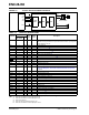
ENC28J60 TABLE 3-2: ENC28J60 CONTROL REGISTER SUMMARY Register Name Bit 7 Bit 6 Bit 5 Bit 4 Bit 3 Bit 2 Bit 1 Bit 0 Value on Reset Details on Page EIE INTIE PKTIE DMAIE LINKIE TXIE r TXERIE RXERIE 0000 0000 65 EIR — PKTIF DMAIF LINKIF TXIF r TXERIF RXERIF -000 0000 66 ESTAT INT BUFER r LATECOL — RXBUSY TXABRT ECON2 AUTOINC PKTDEC PWRSV r VRPS — — — TXRST RXRST DMAST CSUMEN TXRTS RXEN BSEL1 BSEL0 ECON1 ERDPTL ERDPTH EWRPTL EWRPTH ETXSTL ETXSTH ETXND
ENC28J60 TABLE 3-2: ENC28J60 CONTROL REGISTER SUMMARY (CONTINUED) Register Name Bit 7 Bit 6 Bit 5 Bit 4 Bit 3 Bit 2 Bit 1 Bit 0 Value on Reset Details on Page EPMCSL Pattern Match Checksum Low Byte (EPMCS<7:0>) 0000 0000 51 EPMCSH Pattern Match Checksum High Byte (EPMCS<15:0>) 0000 0000 51 EPMOL Pattern Match Offset Low Byte (EPMO<7:0>) EPMOH ERXFCON EPKTCNT — — — UCEN ANDOR CRCEN Pattern Match Offset High Byte (EPMO<12:8>) PMEN MPEN HTEN MCEN BCEN Ethernet Packet Count 0
ENC28J60 3.1.1 ECON1 REGISTER The ECON1 register, shown in Register 3-1, is used to control the main functions of the ENC28J60. Receive enable, transmit request, DMA control and bank select bits can all be found in ECON1.
ENC28J60 3.1.2 ECON2 REGISTER The ECON2 register, shown in Register 3-2, is used to control other main functions of the ENC28J60.
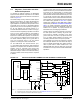
ENC28J60 3.2 Ethernet Buffer 3.2.2 Any space within the 8-Kbyte memory, which is not programmed as part of the receive FIFO buffer, is considered to be the transmit buffer. The responsibility of managing where packets are located in the transmit buffer belongs to the host controller. Whenever the host controller decides to transmit a packet, the ETXST and ETXND Pointers are programmed with addresses specifying where, within the transmit buffer, the particular packet to transmit is located.
ENC28J60 FIGURE 3-2: ETHERNET BUFFER ORGANIZATION Transmit Buffer Start (ETXSTH:ETXSTL) 0000h Buffer Write Pointer (EWRPTH:EWRPTL) Transmit Buffer Data AAh (WBM AAh) Transmit Transmit Buffer End (ETXNDH:ETXNDL) Buffer Receive Buffer Start (ERXSTH:ERXSTL) Receive Buffer (Circular FIFO) Buffer Read Pointer (ERDPTH:ERDPTL) Receive Buffer Data (RBM 55h) 55h Receive Buffer End 1FFFh (ERXNDH:ERXNDL) DS39662E-page 18 . 2006-2012 Microchip Technology Inc.
ENC28J60 3.3 PHY Registers To write to a PHY register: The PHY registers provide configuration and control of the PHY module, as well as status information about its operation. All PHY registers are 16 bits in width. There are a total of 32 PHY addresses; however, only 9 locations are implemented. Writes to unimplemented locations are ignored and any attempts to read these locations will return ‘0’. All reserved locations should be written as ‘0’; their contents should be ignored when read. 1.
Addr Name ENC28J60 PHY REGISTER SUMMARY Bit 15 Bit 14 Bit 12 Bit 11 Bit 10 Bit 9 Bit 8 Bit 7 Bit 6 Bit 5 Bit 4 Bit 3 Bit 2 Bit 1 Bit 0 Reset Values — — PPWRSV r — PDPXMD(1) r — — — — — — — 00-- 00-q 0--- ---- — PFDPX PHDPX — — — — — — — — — ---1 1--- ---- -00- PHCON1 01h PHSTAT1 02h PHID1 03h PHID2 10h PHCON2 — FRCLNK TXDIS 11h PHSTAT2 — — TXSTAT 12h PHIE r r r r 13h PHIR r r r r r r r r 14h PHLCON r r r r LACFG3 LACFG2 L
ENC28J60 REGISTER 3-3: MICMD: MII COMMAND REGISTER U-0 U-0 U-0 U-0 U-0 U-0 R/W-0 R/W-0 — — — — — — MIISCAN MIIRD bit 7 bit 0 Legend: R = Readable bit W = Writable bit U = Unimplemented bit, read as ‘0’ -n = Value at POR ‘1’ = Bit is set ‘0’ = Bit is cleared x = Bit is unknown bit 7-2 Unimplemented: Read as ‘0’ bit 1 MIISCAN: MII Scan Enable bit 1 = PHY register at MIREGADR is continuously read and the data is placed in MIRD 0 = No MII Management scan operation is in progress b
ENC28J60 3.3.4 PHSTAT REGISTERS 3.3.5 PHID1 AND PHID2 REGISTERS The PHSTAT1 and PHSTAT2 registers contain readonly bits that show the current status of the PHY module’s operations, particularly the conditions of the communications link to the rest of the network. The PHID1 and PHID2 registers are read-only registers. They hold constant data that helps identify the Ethernet controller and may be useful for debugging purposes.
ENC28J60 REGISTER 3-5: PHSTAT1: PHYSICAL LAYER STATUS REGISTER 1 U-0 U-0 U-0 R-1 R-1 U-0 U-0 U-0 — — — PFDPX PHDPX — — — bit 15 bit 8 U-0 U-0 U-0 U-0 U-0 R/LL-0 R/LH-0 U-0 — — — — — LLSTAT JBSTAT — bit 7 bit 0 Legend: 1 = Bit is set R = Read-only bit 0 = Bit is cleared U = Unimplemented bit, read as ‘0’ -n = Value at POR R/LH = Read-only latch bit R/LL = Bit latches low LH = Bit latches high bit 15-13 Unimplemented: Read as ‘0’ bit 12 PFDPX: PHY Full-Duplex
ENC28J60 REGISTER 3-6: PHSTAT2: PHYSICAL LAYER STATUS REGISTER 2 U-0 U-0 R-0 R-0 R-0 R-0 R-x U-0 — — TXSTAT RXSTAT COLSTAT LSTAT DPXSTAT(1) — bit 15 bit 8 U-0 U-0 R-0 U-0 U-0 U-0 U-0 U-0 — — PLRITY — — — — — bit 7 bit 0 Legend: R = Readable bit W = Writable bit U = Unimplemented bit, read as ‘0’ -n = Value at POR ‘1’ = Bit is set ‘0’ = Bit is cleared x = Bit is unknown bit 15-14 Unimplemented: Read as ‘0’ bit 13 TXSTAT: PHY Transmit Status bit 1 = PHY is trans
ENC28J60 4.0 SERIAL PERIPHERAL INTERFACE (SPI) 4.1 Overview Commands and data are sent to the device via the SI pin, with data being clocked in on the rising edge of SCK. Data is driven out by the ENC28J60 on the SO line, on the falling edge of SCK. The CS pin must be held low while any operation is performed and returned high when finished. The ENC28J60 is designed to interface directly with the Serial Peripheral Interface (SPI) port available on many microcontrollers.
ENC28J60 4.2 SPI Instruction Set followed by a 5-bit argument that specifies either a register address or a data constant. Write and bit field instructions are also followed by one or more bytes of data. The operation of the ENC28J60 depends entirely on commands given by an external host controller over the SPI interface. These commands take the form of instructions, of one or more bytes, which are used to access the control memory and Ethernet buffer spaces.
ENC28J60 4.2.1 READ CONTROL REGISTER COMMAND registers in the current bank. If the 5-bit address is an ETH register, then data in the selected register will immediately start shifting out MSb first on the SO pin. Figure 4-3 shows the read sequence for these registers. The Read Control Register (RCR) command allows the host controller to read any of the ETH, MAC and MII registers in any order. The contents of the PHY registers are read via a special MII register interface (see Section 3.3.
ENC28J60 4.2.2 READ BUFFER MEMORY COMMAND 4.2.3 The Read Buffer Memory (RBM) command allows the host controller to read bytes from the integrated 8-Kbyte transmit and receive buffer memory. The Write Control Register (WCR) command allows the host controller to write to any of the ETH, MAC and MII Control registers in any order. The PHY registers are written to via a special MII register interface (see Section 3.3.2 “Writing PHY Registers” for more information).
ENC28J60 4.2.4 WRITE BUFFER MEMORY COMMAND The BFS command is started by pulling the CS pin low. The BFS opcode is then sent, followed by a 5-bit address (A4 through A0). The 5-bit address identifies any of the ETH registers in the current bank. After the BFS command and address are sent, the data byte containing the bit field set information should be sent, MSb first. The supplied data will be logically ORed to the content of the addressed register on the rising edge of the SCK line for the D0 bit.
ENC28J60 4.2.7 SYSTEM RESET COMMAND The command is started by pulling the CS pin low. The SRC opcode is the sent, followed by a 5-bit Soft Reset command constant of 1Fh. The SRC operation is terminated by raising the CS pin. The System Reset Command (SRC) allows the host controller to issue a System Soft Reset command. Unlike other SPI commands, the SRC is only a single byte command and does not operate on any register.
ENC28J60 5.0 ETHERNET OVERVIEW beginning of the Ethernet packet. Thus, traffic seen on the twisted-pair cabling will appear as shown in Figure 5-1. Before discussing the use of the ENC28J60 as an Ethernet interface, it may be helpful to review the structure of a typical data frame. Users requiring more information should refer to the IEEE 802.3 standard which is the basis for the Ethernet protocol. 5.1 5.1.
ENC28J60 5.1.2 DESTINATION ADDRESS 5.1.5 The destination address field is a 6-byte field filled with the MAC address of the device that the packet is directed to. If the Least Significant bit in the first byte of the MAC address is set, the address is a Multicast destination. For example, 01-00-00-00-F0-00 and 33-45-67-89-AB-CD are Multicast addresses, while 00-00-00-00-F0-00 and 32-45-67-89-AB-CD are not. The data field is a variable length field, anywhere from 0 to 1500 bytes.
ENC28J60 6.0 INITIALIZATION 6.2 All memory which is not used by the receive buffer is considered the transmission buffer. Data which is to be transmitted should be written into any unused space. After a packet is transmitted, however, the hardware will write a seven-byte status vector into memory after the last byte in the packet. Therefore, the host controller should leave at least seven bytes between each packet and the beginning of the receive buffer.
ENC28J60 6.5 MAC Initialization Settings 4. Several of the MAC registers require configuration during initialization. This only needs to be done once; the order of programming is unimportant. 1. 2. 3. Set the MARXEN bit in MACON1 to enable the MAC to receive frames. If using full duplex, most applications should also set TXPAUS and RXPAUS to allow IEEE defined flow control to function. Configure the PADCFG, TXCRCEN and FULDPX bits of MACON3.
ENC28J60 REGISTER 6-2: MACON3: MAC CONTROL REGISTER 3 R/W-0 R/W-0 R/W-0 R/W-0 R/W-0 R/W-0 R/W-0 R/W-0 PADCFG2 PADCFG1 PADCFG0 TXCRCEN PHDREN HFRMEN FRMLNEN FULDPX bit 7 bit 0 Legend: R = Readable bit W = Writable bit U = Unimplemented bit, read as ‘0’ -n = Value at POR ‘1’ = Bit is set ‘0’ = Bit is cleared x = Bit is unknown bit 7-5 PADCFG<2:0>: Automatic Pad and CRC Configuration bits 111 = All short frames will be zero-padded to 64 bytes and a valid CRC will then be appended 11
ENC28J60 REGISTER 6-3: MACON4: MAC CONTROL REGISTER 4 U-0 R/W-0 R/W-0 R/W-0 U-0 U-0 R-0 R-0 — DEFER BPEN NOBKOFF — — r r bit 7 bit 0 Legend: r = Reserved bit R = Readable bit W = Writable bit U = Unimplemented bit, read as ‘0’ -n = Value at POR ‘1’ = Bit is set ‘0’ = Bit is cleared x = Bit is unknown bit 7 Unimplemented: Read as ‘0’ bit 6 DEFER: Defer Transmission Enable bit (applies to half duplex only) 1 = When the medium is occupied, the MAC will wait indefinitely for it t
ENC28J60 6.6 PHY Initialization Settings If using half duplex, the host controller may wish to set the PHCON2.HDLDIS bit to prevent automatic loopback of the data which is transmitted. Depending on the application, bits in three of the PHY module’s registers may also require configuration. The PHY register, PHLCON, controls the outputs of LEDA and LEDB. If an application requires a LED configuration other than the default, PHLCON must be altered to match the new requirements.
ENC28J60 NOTES: DS39662E-page 38 . 2006-2012 Microchip Technology Inc.
ENC28J60 7.0 TRANSMITTING AND RECEIVING PACKETS 7.1 Transmitting Packets Additionally, the ENC28J60 requires a single per packet control byte to precede the packet for transmission. The per packet control byte is organized as shown in Figure 7-1. Before transmitting packets, the MAC registers which alter the transmission characteristics should be initialized as documented in Section 6.0 “Initialization”.
ENC28J60 FIGURE 7-2: SAMPLE TRANSMIT PACKET LAYOUT Buffer Pointers Address Memory ETXST = 0120h 0120h 0Eh 0121h data[1] 0122h data[2] ETXND = 0156h 0156h 0157h 0158h 0159h 015Ah 015Bh 015Ch 015Dh Description Control 015Eh 2. 3. 4. 5. Status Vector Status Vector Written by the Hardware DMA and transmission engine share the same memory access port.
ENC28J60 TABLE 7-1: Bit 55-52 TRANSMIT STATUS VECTORS Field Description Zero 0 51 Transmit VLAN Tagged Frame Frame’s length/type field contained 8100h which is the VLAN protocol identifier. 50 Backpressure Applied Carrier sense method backpressure was previously applied. 49 Transmit Pause Control Frame The frame transmitted was a control frame with a valid pause opcode. 48 Transmit Control Frame The frame transmitted was a control frame.
ENC28J60 TABLE 7-2: Register Name EIE EIR ESTAT ECON1 ETXSTL SUMMARY OF REGISTERS USED FOR PACKET TRANSMISSION Bit 7 Bit 6 Bit 5 Bit 4 Bit 3 Bit 2 Bit 1 Bit 0 Reset Values on page INTIE — PKTIE PKTIF DMAIE DMAIF LINKIE LINKIF TXIE TXIF r r TXERIE TXERIF RXERIE RXERIF 13 13 INT BUFER r LATECOL — RXBUSY TXABRT CLKRDY(1) 13 TXRST RXRST DMAST CSUMEN TXRTS RXEN BSEL1 BSEL0 13 TX Start Low Byte (ETXST<7:0>) ETXSTH — ETXNDL — — 13 TX Start High Byte (ETXST<12:8>) 13 TX
ENC28J60 7.2 Receiving Packets 7.2.1 After reception is enabled, packets which are not filtered out will be written into the circular receive buffer. Any packet which does not meet the necessary filter criteria will be discarded and the host controller will not have any means of identifying that a packet was thrown away. When a packet is accepted and completely written into the buffer, the EPKTCNT register will increment, the EIR.
ENC28J60 TABLE 7-3: RECEIVE STATUS VECTORS Bit Field Description 31 Zero 0 30 Receive VLAN Type Detected Current frame was recognized as a VLAN tagged frame. 29 Receive Unknown Opcode Current frame was recognized as a control frame but it contained an unknown opcode. 28 Receive Pause Control Frame Current frame was recognized as a control frame containing a valid pause frame opcode and a valid destination address.
ENC28J60 7.2.4 FREEING RECEIVE BUFFER SPACE Because only one pointer is available to control buffer area ownership, the host controller must process packets in the order they are received. If the host controller wishes to save a packet to be processed later, it should copy the packet to an unused location in memory. It may accomplish this efficiently using the integrated DMA controller (see Section 13.0 “Direct Memory Access Controller”).
ENC28J60 TABLE 7-4: SUMMARY OF REGISTERS USED FOR PACKET RECEPTION Bit 7 Bit 6 Bit 5 Bit 4 Bit 3 Bit 2 Bit 1 Bit 0 Reset Values on page INTIE — PKTIE PKTIF DMAIE DMAIF LINKIE LINKIF TXIE TXIF r r TXERIE TXERIF RXERIE RXERIF 13 13 ESTAT INT BUFER r LATECOL — RXBUSY TXABRT CLKRDY(1) 13 ECON2 AUTOINC PKTDEC PWRSV r VRPS — — — 13 ECON1 TXRST RXRST DMAST CSUMEN TXRTS RXEN BSEL1 BSEL0 13 Register Name EIE EIR ERXSTL RX Start Low Byte (ERXST<7:0>) ERXSTH — ERXN
ENC28J60 8.0 RECEIVE FILTERS The individual filters are all configured by the ERXFCON register (Register 8-1). More than one filter can be active at any given time. Additionally, the filters can be configured by the ANDOR bit to either logically AND, or logically OR, the tests of several filters. In other words, the filters may be set so that only packets accepted by all active filters are accepted, or a packet accepted by any one filter is accepted.
ENC28J60 REGISTER 8-1: R/W-1 UCEN bit 7 R/W-0 ANDOR Legend: R = Readable bit -n = Value at POR bit 7 bit 6 bit 5 bit 4 bit 3 bit 2 bit 1 bit 0 ERXFCON: ETHERNET RECEIVE FILTER CONTROL REGISTER R/W-1 CRCEN R/W-0 PMEN R/W-0 MPEN W = Writable bit ‘1’ = Bit is set R/W-0 HTEN R/W-0 MCEN R/W-1 BCEN bit 0 U = Unimplemented bit, read as ‘0’ ‘0’ = Bit is cleared x = Bit is unknown UCEN: Unicast Filter Enable bit When ANDOR = 1: 1 = Packets not having a destination address matching the local MAC add
ENC28J60 FIGURE 8-1: RECEIVE FILTERING USING OR LOGIC Packet Detected on Wire, ANDOR = 0 (OR) UCEN, PMEN, MPEN, HTEN, MCEN and BCEN all clear? Yes No UCEN set? Yes No PMEN set? Unicast packet? Yes CRCEN set? Yes No Yes No Pattern matches? No CRCEN valid? Yes Yes Accept Packet No No Reject Packet MPEN set? Yes No HTEN set? Yes Hash table bit set? Yes No Yes Multicast destination? Yes No No BCEN set? Yes No No MCEN set? Magic Packet™ for us? Yes No 2006-2012 Mi
ENC28J60 FIGURE 8-2: RECEIVE FILTERING USING AND LOGIC Packet Detected on Wire ANDOR = 1 (AND) UCEN set? Yes No Unicast packet? No Yes PMEN set? Yes Pattern matches? No No Yes MPEN set? Yes Magic Packet™ for us? No No Yes HTEN set? Yes Hash Table bit set? No No Yes MCEN set? Yes Multicast destination? No No Yes BCEN set? Yes Broadcast destination? No No Yes No CRCEN set? Yes No CRC valid? Yes Accept Packet DS39662E-page 50 .
ENC28J60 8.1 Unicast Filter the filter criteria will immediately not be met, even if the corresponding mask bits are all ‘0’. The Pattern Match Checksum registers should be programmed to the checksum which is expected for the selected bytes. The checksum is calculated in the same manner that the DMA module calculates checksums (see Section 13.2 “Checksum Calculations”).
ENC28J60 8.3 Magic Packet™ Filter within it, then the packet will meet the Magic Packet filter criteria. The Magic Packet pattern consists of a sync pattern of six 0xFF bytes, followed by 16 repeats of the destination address. See Figure 8-4 for a sample Magic Packet. The Magic Packet filter checks the destination address and data fields of all incoming packets.
ENC28J60 9.0 DUPLEX MODE CONFIGURATION AND NEGOTIATION 2. The ENC28J60 does not support automatic duplex negotiation. If it is connected to an automatic duplex negotiation enabled network switch or Ethernet controller, the ENC28J60 will be detected as a half-duplex device. To communicate in Full-Duplex mode, the ENC28J60 and the remote node (switch, router or Ethernet controller) must be manually configured for full-duplex operation. 9.
ENC28J60 NOTES: DS39662E-page 54 . 2006-2012 Microchip Technology Inc.
ENC28J60 10.0 matically decrement every 512 bit times or 51.2 s. While the timer is counting down, reception of packets is still enabled. If new pause frames arrive, the timer will be reinitialized with the new pause timer value. When the timer reaches zero or was sent a frame with a zero pause timer value, the MAC that received the pause frame will resume transmitting any pending packets.
ENC28J60 To enable flow control on the ENC28J60 in Full-Duplex mode, the host controller must set the TXPAUS and RXPAUS bits in the MACON1 register. Then, at any time that the receiver buffer is running out of space, the host controller should turn flow control on by writing the value 02h to the EFLOCON register. The hardware will periodically transmit pause frames loaded with the pause timer value specified in the EPAUS registers.
ENC28J60 TABLE 10-1: Name SUMMARY OF REGISTERS USED WITH FLOW CONTROL Bit 7 Bit 6 Bit 5 Bit 4 Bit 3 Bit 2 TXRST RXRST DMAST CSUMEN TXRTS RXEN MACON1 — — — r TXPAUS RXPAUS MABBIPG — ECON1 EFLOCON — Bit 1 Bit 0 Reset Values on page BSEL1 BSEL0 13 PASSALL MARXEN Back-to-Back Inter-Packet Gap (BBIPG<6:0>) — — — — 14 14 FULDPXS FCEN1 FCEN0 14 EPAUSL Pause Timer Value Low Byte (EPAUS<7:0>) 14 EPAUSH Pause Timer Value High Byte (EPAUS<15:8>) 14 Legend: r = reserved, —
ENC28J60 NOTES: DS39662E-page 58 . 2006-2012 Microchip Technology Inc.
ENC28J60 11.0 RESET The ENC28J60 differentiates between various kinds of Reset: • • • • • Power-on Reset (POR) System Reset Transmit Only Reset Receive Only Reset Miscellaneous MAC and PHY Subsystem Resets A simplified block diagram of the On-Chip Reset Circuit is shown in Figure 11-1. FIGURE 11-1: ON-CHIP RESET CIRCUIT Soft Reset Command Hardware Reset System Reset POR Reset Host Interface Reset Transmit Transmit Reset Reset Receive Receive Reset 2006-2012 Microchip Technology Inc. .
ENC28J60 11.1 Power-on Reset (POR) After a System Reset, all PHY registers should not be read or written to until at least 50 s have passed since the Reset has ended. All registers will revert to their Reset default values. The dual port buffer memory will maintain state throughout the System Reset. A Power-on Reset pulse is generated on-chip whenever VDD rises above a certain threshold. This allows the device to start in the initialized state when VDD is adequate for operation. 11.
ENC28J60 11.5 PHY Subsystem Reset Unlike other Resets, the PHY cannot be removed from Reset immediately after setting PRST. The PHY requires a delay, after which the hardware automatically clears the PRST bit. After a Reset is issued, the host controller should poll PRST and wait for it to become clear before using the PHY. The PHY module may be reset by writing a ‘1’ to the PRST bit in the PHCON1 register (Register 11-1). All the PHY register contents will revert to their Reset defaults.
ENC28J60 NOTES: DS39662E-page 62 . 2006-2012 Microchip Technology Inc.
ENC28J60 12.0 INTERRUPTS When an enabled interrupt occurs, the interrupt pin will remain low until all flags which are causing the interrupt are cleared or masked off (enable bit is cleared) by the host controller. If more than one interrupt source is enabled, the host controller must poll each flag in the EIR register to determine the source(s) of the interrupt.
ENC28J60 12.1 INT Interrupt Enable (INTIE) When any of the above interrupts are enabled and generated, the virtual bit, INT in the ESTAT register (Register 12-1), will be set to ‘1’. If EIE.INTIE is ‘1’, the INT pin will be driven low. The INT Interrupt Enable bit (INTIE) is a global enable bit which allows the following interrupts to drive the INT pin: • • • • • • 12.1.
ENC28J60 REGISTER 12-2: EIE: ETHERNET INTERRUPT ENABLE REGISTER R/W-0 R/W-0 R/W-0 R/W-0 R/W-0 R/W-0 R/W-0 R/W-0 INTIE PKTIE DMAIE LINKIE TXIE r TXERIE RXERIE bit 7 bit 0 Legend: r = Reserved bit R = Readable bit W = Writable bit U = Unimplemented bit, read as ‘0’ -n = Value at POR ‘1’ = Bit is set ‘0’ = Bit is cleared bit 7 INTIE: Global INT Interrupt Enable bit 1 = Allow interrupt events to drive the INT pin 0 = Disable all INT pin activity (pin is continuously driven high) bi
ENC28J60 REGISTER 12-3: EIR: ETHERNET INTERRUPT REQUEST (FLAG) REGISTER U-0 R-0 R/C-0 R-0 R/C-0 R-0 R/C-0 R/C-0 — PKTIF DMAIF LINKIF TXIF r TXERIF RXERIF bit 7 bit 0 Legend: r = Reserved bit R = Readable bit C = Clearable bit U = Unimplemented bit, read as ‘0’ -n = Value at POR ‘1’ = Bit is set ‘0’ = Bit is cleared x = Bit is unknown bit 7 Unimplemented: Read as ‘0’ bit 6 PKTIF: Receive Packet Pending Interrupt Flag bit 1 = Receive buffer contains one or more unprocessed pack
ENC28J60 REGISTER 12-4: PHIE: PHY INTERRUPT ENABLE REGISTER R-0 R-0 R-0 R-0 R-0 R-0 R-0 R-0 r r r r r r r r bit 15 bit 8 R-0 R-0 R/W-0 R/W-0 R-0 R-0 R/W-0 R/W-0 r r r PLNKIE r r PGEIE r bit 7 bit 0 Legend: r = Reserved bit R = Readable bit W = Writable bit U = Unimplemented bit, read as ‘0’ -n = Value at POR ‘1’ = Bit is set ‘0’ = Bit is cleared bit 15-6 Reserved: Write as ‘0’, ignore on read bit 5 Reserved: Maintain as ‘0’ bit 4 PLNKIE: PHY Link Change Int
ENC28J60 12.1.2 RECEIVE ERROR INTERRUPT FLAG (RXERIF) Upon any of these conditions, the EIR.TXERIF flag is set to ‘1’. Once set, it can only be cleared by the host controller or by a Reset condition. If the transmit error interrupt is enabled (EIE.TXERIE = 1 and EIE.INTIE = 1), an interrupt is generated by driving the INT pin low until the interrupt flag or interrupt enable is cleared. If the transmit error interrupt is not enabled (EIE.TXERIE = 0 or EIE.
ENC28J60 12.1.5 LINK CHANGE INTERRUPT FLAG (LINKIF) 12.1.6 DMA INTERRUPT FLAG (DMAIF) The DMA interrupt indicates that the DMA module has completed its memory copy or checksum calculation (ECON1.DMAST has transitioned from ‘1’ to ‘0’). Additionally, this interrupt will be caused if the host controller cancels a DMA operation by manually clearing the DMAST bit. Once set, DMAIF can only be cleared by the host controller or by a Reset condition. If the DMA interrupt is enabled (EIE.DMAIE = 1 and EIE.
ENC28J60 12.2 Wake-On-LAN/Remote Wake-up 12.2.1 Wake-On-LAN or Remote Wake-up is useful in conserving system power. The host controller and other subsystems can be put in Low-Power mode and be woken up by the ENC28J60 when a wake-up packet is received from a remote station. The ENC28J60 must not be in Power-Save mode and the transmit and receive modules must be enabled in order to receive a wake-up packet.
ENC28J60 13.0 DIRECT MEMORY ACCESS CONTROLLER 13.1 To copy memory within the buffer: The ENC28J60 incorporates a dual purpose DMA controller which can be used to copy data between locations within the 8-Kbyte memory buffer. It can also be used to calculate a 16-bit checksum which is compatible with various industry standard protocols, including TCP and IP. 1. When a DMA operation begins, the EDMAST register pair is copied into an Internal Source Pointer.
ENC28J60 13.2 Checksum Calculations Pointers will not be modified and no memory will be written to. The EDMACSH and EDMACSL registers will contain the calculated checksum. The host controller may write this value into a packet, compare this value with a received checksum, or use it for other purposes. The checksum calculation logic treats the source data as a series of 16-bit big-endian integers.
ENC28J60 14.0 POWER-DOWN When normal operation is desired, the host controller must perform a slightly modified procedure: The ENC28J60 may be commanded to power-down via the SPI interface. When powered down, it will no longer be able to transmit and receive any packets. 1. 2. To maximize power savings: 1. 2. 3. 4. 5. Turn off packet reception by clearing ECON1.RXEN. Wait for any in-progress packets to finish being received by polling ESTAT.RXBUSY. This bit should be clear before proceeding.
ENC28J60 NOTES: DS39662E-page 74 . 2006-2012 Microchip Technology Inc.
ENC28J60 15.0 BUILT-IN SELF-TEST CONTROLLER The BIST controller is operated through four registers: • EBSTCON register (control and status register) • EBSTSD register (fill seed/initial shift value) • EBSTCSH and EBSTCSL registers (high and low bytes of generated checksum) The ENC28J60 features a Built-in Self-Test (BIST) module which is designed to confirm proper operation of each bit in the 8-Kbyte memory buffer.
ENC28J60 15.1 Using the BIST At any time during a test, the test can be canceled by clearing the BISTST, DMAST and TME bits. While the BIST is filling memory, the EBSTSD register should not be accessed, nor should any configuration changes occur. When the BIST completes its memory fill and checksum generation, the BISTST bit will automatically be cleared.
ENC28J60 TABLE 15-1: Name ECON1 ERXNDL ERXNDH EDMASTL EDMASTH EDMANDL EDMANDH SUMMARY OF REGISTERS ASSOCIATED WITH THE SELF-TEST CONTROLLER Bit 7 Bit 6 Bit 5 Bit 4 Bit 3 Bit 2 Bit 1 Bit 0 Reset Values on page TXRST RXRST DMAST CSUMEN TXRTS RXEN BSEL1 BSEL0 13 RX End Low Byte (ERXND<7:0>) — — — RX End High Byte (ERXND<12:8>) DMA Start Low Byte (EDMAST<7:0>) — — — 13 13 13 DMA Start High Byte (EDMAST<12:8>) 13 DMA End Low Byte (EDMAND<7:0>) — — — 13 DMA End High Byte (EDMAND<12:8>
ENC28J60 NOTES: DS39662E-page 78 . 2006-2012 Microchip Technology Inc.
ENC28J60 16.0 ELECTRICAL CHARACTERISTICS Absolute Maximum Ratings Storage temperature ...............................................................................................................................-65°C to +150°C Ambient temperature under bias............................................................................................. -40°C to +85°C (Industrial) 0°C to +70°C (Commercial) Voltage on VDD, VDDOSC, VDDPLL, VDDRX and VDDTX, with respect to VSS ..................................
ENC28J60 16.1 DC Characteristics: ENC28J60 (Industrial and Commercial) DC CHARACTERISTICS Param. No. Sym Characteristic D001 VDD Supply Voltage D002 VPOR VDD Power-on Reset Voltage D003 SVDD VDD Rise Rate to Ensure Internal Power-on Reset Signal VIH Input High Voltage D004 SCK, CS, SI, RESET D005 OSC1 VIL Standard Operating Conditions -40°C TA +85°C, 3.10V VDD 3.60V (Industrial) 0°C TA +70°C, 3.10V VDD 3.60V (Commercial) Min Typ Max Units Conditions 3.10 3.30 3.
ENC28J60 TABLE 16-1: AC CHARACTERISTICS: ENC28J60 (INDUSTRIAL AND COMMERCIAL) Standard Operating Conditions -40°C TA +85°C, 3.10V VDD 3.60V (Industrial) 0°C TA +70°C, 3.10V VDD 3.60V (Commercial) AC CHARACTERISTICS TABLE 16-2: Param. No. OSCILLATOR TIMING CHARACTERISTICS Sym Min Max Units 25 25 MHz FOSC Clock In Frequency TOSC Clock In Period 40 40 ns TDUTY Duty Cycle (external clock input) 40 60 % f Clock Tolerance — 50 ppm Min Max Units TABLE 16-3: Param.
ENC28J60 FIGURE 16-1: SPI INPUT TIMING TCSS TCSH TCSD CS SCK TSU THD MSb In SI LSb In 1/FSCK SO High-Impedance FIGURE 16-2: SPI OUTPUT TIMING CS SCK TV SO TDIS TV MSb Out LSb Out 1/FSCK SI LSb In Don’t Care TABLE 16-6: Param. No.
ENC28J60 17.0 PACKAGING INFORMATION 17.1 Package Marking Information 28-Lead SPDIP Example ENC28J60-I/SP e3 1210017 XXXXXXXXXXXXXXXXX XXXXXXXXXXXXXXXXX YYWWNNN 28-Lead SOIC Example XXXXXXXXXXXXXXXXXXXX XXXXXXXXXXXXXXXXXXXX XXXXXXXXXXXXXXXXXXXX YYWWNNN ENC28J60-I/SO e3 1210017 28-Lead SSOP Example XXXXXXXXXXXX XXXXXXXXXXXX YYWWNNN ENC28J60 /SS e3 1210017 28-Lead QFN Example XXXXXXXX XXXXXXXX YYWWNNN ENC28J60 -I/ML e3 1210017 Legend: XX...
ENC28J60 17.2 Package Details The following sections give the technical details of the packages.
ENC28J60 Note: For the most current package drawings, please see the Microchip Packaging Specification located at http://www.microchip.com/packaging 2006-2012 Microchip Technology Inc. .
ENC28J60 Note: For the most current package drawings, please see the Microchip Packaging Specification located at http://www.microchip.com/packaging DS39662E-page 86 . 2006-2012 Microchip Technology Inc.
ENC28J60 Note: For the most current package drawings, please see the Microchip Packaging Specification located at http://www.microchip.com/packaging 2006-2012 Microchip Technology Inc. .
ENC28J60 /HDG 3ODVWLF 6KULQN 6PDOO 2XWOLQH 66 ± PP %RG\ >6623@ 1RWH )RU WKH PRVW FXUUHQW SDFNDJH GUDZLQJV SOHDVH VHH WKH 0LFURFKLS 3DFNDJLQJ 6SHFLILFDWLRQ ORFDWHG DW KWWS ZZZ PLFURFKLS FRP SDFNDJLQJ D N E E1 1 2 NOTE 1 b e c A2 A φ A1 L L1 8QLWV 'LPHQVLRQ /LPLWV 1XPEHU RI 3LQV 0,//,0(7(56 0,1 1 120 0$; 3LWFK H 2YHUDOO +HLJKW $ ± %6& ± 0ROGHG 3DFNDJH 7KLFNQHVV $ 6WDQGRII $ ± ± 2YHUDOO :LGWK ( 0ROGHG 3DFNDJ
ENC28J60 Note: For the most current package drawings, please see the Microchip Packaging Specification located at http://www.microchip.com/packaging 2006-2012 Microchip Technology Inc. .
ENC28J60 DS39662E-page 90 . 2006-2012 Microchip Technology Inc.
ENC28J60 2006-2012 Microchip Technology Inc. .
ENC28J60 /HDG 3ODVWLF 4XDG )ODW 1R /HDG 3DFNDJH 0/ ± [ PP %RG\ >4)1@ ZLWK PP &RQWDFW /HQJWK 1RWH )RU WKH PRVW FXUUHQW SDFNDJH GUDZLQJV SOHDVH VHH WKH 0LFURFKLS 3DFNDJLQJ 6SHFLILFDWLRQ ORFDWHG DW KWWS ZZZ PLFURFKLS FRP SDFNDJLQJ DS39662E-page 92 . 2006-2012 Microchip Technology Inc.
ENC28J60 APPENDIX A: REVISION HISTORY Revision A (January 2006) Original data sheet for the ENC28J60. Revision B (July 2006) Minor edits and format changes throughout the document. Revision C (January 2008) Added one line to the “Ethernet Controller Features” section and added omitted revision history. Minor edits to text throughout document. Revision D (July 2012) Updated package drawings in Section 17.
ENC28J60 NOTES: DS39662E-page 94 . 2006-2012 Microchip Technology Inc.
ENC28J60 THE MICROCHIP WEB SITE CUSTOMER SUPPORT Microchip provides online support via our WWW site at www.microchip.com. This web site is used as a means to make files and information easily available to customers.
ENC28J60 READER RESPONSE It is our intention to provide you with the best documentation possible to ensure successful use of your Microchip product. If you wish to provide your comments on organization, clarity, subject matter, and ways in which our documentation can better serve you, please FAX your comments to the Technical Publications Manager at (480) 792-4150. Please list the following information, and use this outline to provide us with your comments about this document.
ENC28J60 INDEX A Ethernet Packet Format ............................................................ 31 CRC Field ........................................................... 32 Data Field ........................................................... 32 Destination Address ........................................... 32 Padding Field ..................................................... 32 Preamble/Start-of-Frame Delimiter..................... 31 Source Address .................................................
ENC28J60 O MICMD (MII Command).............................................. 21 MISTAT (MII Status) ................................................... 21 PHCON1 (PHY Control 1) .......................................... 61 PHCON2 (PHY Control 2) .......................................... 37 PHID (PHY Device ID)................................................ 22 PHIE (PHY Interrupt Enable) ...................................... 67 PHIR (PHY Interrupt Request, Flag)...........................
ENC28J60 PRODUCT IDENTIFICATION SYSTEM To order or obtain information, e.g., on pricing or delivery, refer to the factory or the listed sales office. PART NO.
ENC28J60 NOTES: DS39662E-page 100 . 2006-2012 Microchip Technology Inc.
Note the following details of the code protection feature on Microchip devices: • Microchip products meet the specification contained in their particular Microchip Data Sheet. • Microchip believes that its family of products is one of the most secure families of its kind on the market today, when used in the intended manner and under normal conditions. • There are dishonest and possibly illegal methods used to breach the code protection feature.
Worldwide Sales and Service AMERICAS ASIA/PACIFIC ASIA/PACIFIC EUROPE Corporate Office 2355 West Chandler Blvd. Chandler, AZ 85224-6199 Tel: 480-792-7200 Fax: 480-792-7277 Technical Support: http://www.microchip.com/ support Web Address: www.microchip.