
Datasheet


2006-2012 Microchip Technology Inc. . DS39662E-page 5
ENC28J60
2.0 EXTERNAL CONNECTIONS
2.1 Oscillator
The ENC28J60 is designed to operate at 25 MHz with a
crystal connected to the OSC1 and OSC2 pins. The
ENC28J60 design requires the use of a parallel reso-
nance crystal. Use of a series resonance crystal may give
a frequency out of the crystal manufacturer specifications.
A typical oscillator circuit is shown in Figure 2-1.
The ENC28J60 may also be driven by an external clock
source connected to the OSC1 pin as shown in
Figure 2-2.
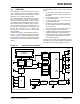
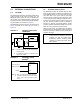
FIGURE 2-1: CRYSTAL OSCILLATOR
OPERATION
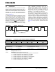
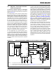
FIGURE 2-2: EXTERNAL CLOCK
SOURCE
(1)
2.2 Oscillator Start-up Timer
The ENC28J60 contains an Oscillator Start-up Timer
(OST) to ensure that the oscillator and integrated PHY
have stabilized before use. The OST does not expire
until 7500 OSC1 clock cycles (300 s) pass after
Power-on Reset or wake-up from Power-Down mode
occurs. During the delay, all Ethernet registers and buf-
fer memory may still be read and written to through the
SPI bus. However, software should not attempt to
transmit any packets (set ECON1.TXRTS), enable
reception of packets (set ECON1.RXEN) or access any
MAC, MII or PHY registers during this period.
When the OST expires, the CLKRDY bit in the ESTAT
register will be set. The application software should poll
this bit as necessary to determine when normal device
operation can begin.
C
1
C
2
XTAL
OSC2
R
S
(1)
OSC1
RF
(2)
To Internal Logic
Note 1: A series resistor, RS, may be required for AT
strip cut crystals.
2: The feedback resistor, R
F , is typically in the
range of 2 to 10 M.
ENC28J60
3.3V Clock from
External System
OSC1
OSC2
Open
(2)
Note 1: Duty cycle restrictions must be observed.
2: A resistor to ground may be used to reduce
system noise. This may increase system
current.
ENC28J60
Note: After a Power-on Reset, or the ENC28J60
is removed from Power-Down mode, the
CLKRDY bit must be polled before
transmitting packets, enabling packet
reception or accessing any MAC, MII or
PHY registers.