
Specifications
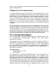
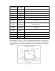


27
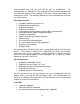
Pin Name
Pin Type
Pin Description
AV
DD
Power
Positive supply for analog modules.
AV
SS
Power
Ground reference for analog modules
V
DD
Power
Positive supply for peripheral logic and I/O pins
V
SS
Power
Ground reference for logic and I/O pins
V
CAP
/V
DDCORE
Power
CPU logic filter capacitor connection
MCLR
Input/Power
Master Clear (Reset) input. This pin is an active
low reset.
PGEC1
Input/Output
Clock input pin for programming/debugging
comm channel 1
PGED1
Input/Output
Data I/O pin for programming/debugging comm
channel 1
OSC1
Input
Oscillator crystal input
OSC2
Input/Output
Oscillator crystal output
V
REF
+
Input
Analog voltage reference (high) input
V
REF
-
Input
Analog voltage reference (low) input
Table 3 Pins to be connected at all times
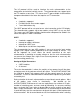
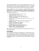
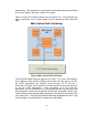
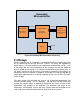
Also required at all times is the use of decoupling capacitors on every pair of
power supply pins. Our printed circuit board design will include these capacitors
as well as the resistors pictured. A diagram of this configuration is shown below
in Figure 7.
Figure 7 Required Minimum Connections