
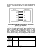
Specifications

79
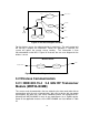
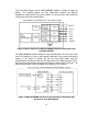
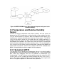
The main block diagram for the MRF24WB0MA module is shown in Figure 36
below. This diagram depicts the main connections between the different
components within the RF transceiver module. The arrows on the right show how
it will connect with the microcontroller.
Figure 36 Block Diagram for MRF24WB0MA (Reprinted with permission
from MicroChip®)
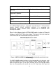
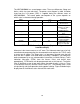
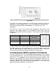
The MRF24WB0MA module interfaces to the microcontroller via a four-wire serial
slave SPI interface, as well as the interrupt, hibernate, reset, power and ground
signals. In the Figure 37 below, we can see that input/ output from the
microcontroller will connect with the SPI Chip Select (CS) input and clock (SCK),
while the data will exchange through the SPI data in and out (SDI, SDO) pins. All
data communications with the module are through the SPI interface.
Figure 37 MRF24WB0MA interface to microcontroller (Reprinted with
permission from MicroChip®)