
Datasheet
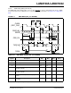

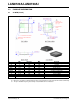
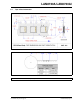
Table Of Contents
- Small Footprint RMII 10/100 Ethernet Transceiver with HP Auto-MDIX Support
- 1.0 Introduction
- 2.0 Pin Description and Configuration
- 3.0 Functional Description
- 3.1 Transceiver
- 3.2 Auto-negotiation
- 3.3 HP Auto-MDIX Support
- 3.4 MAC Interface
- 3.5 Serial Management Interface (SMI)
- 3.6 Interrupt Management
- 3.7 Configuration Straps
- 3.8 Miscellaneous Functions
- 3.9 Application Diagrams
- 4.0 Register Descriptions
- 4.1 Register Nomenclature
- 4.2 Control and Status Registers
- TABLE 4-2: SMI Register Map
- 4.2.1 Basic Control Register
- 4.2.2 Basic Status Register
- 4.2.3 PHY Identifier 1 Register
- 4.2.4 PHY Identifier 2 Register
- 4.2.5 Auto Negotiation Advertisement Register
- 4.2.6 Auto Negotiation Link Partner Ability Register
- 4.2.7 Auto Negotiation Expansion Register
- 4.2.8 Mode Control/Status Register
- 4.2.9 Special Modes Register
- 4.2.10 Symbol Error Counter Register
- 4.2.11 Special Control/Status Indications Register
- 4.2.12 Interrupt Source Flag Register
- 4.2.13 Interrupt Mask Register
- 4.2.14 PHY Special Control/Status Register
- 5.0 Operational Characteristics
- 6.0 Package Information
- 7.0 Application Notes
- Appendix A: Data Sheet Revision History
- The Microchip Web Site
- Customer Change Notification Service
- Customer Support
- Product Identification System
- Worldwide Sales and Service
2016 Microchip Technology Inc. DS00002165B-page 61
LAN8720A/LAN8720AI
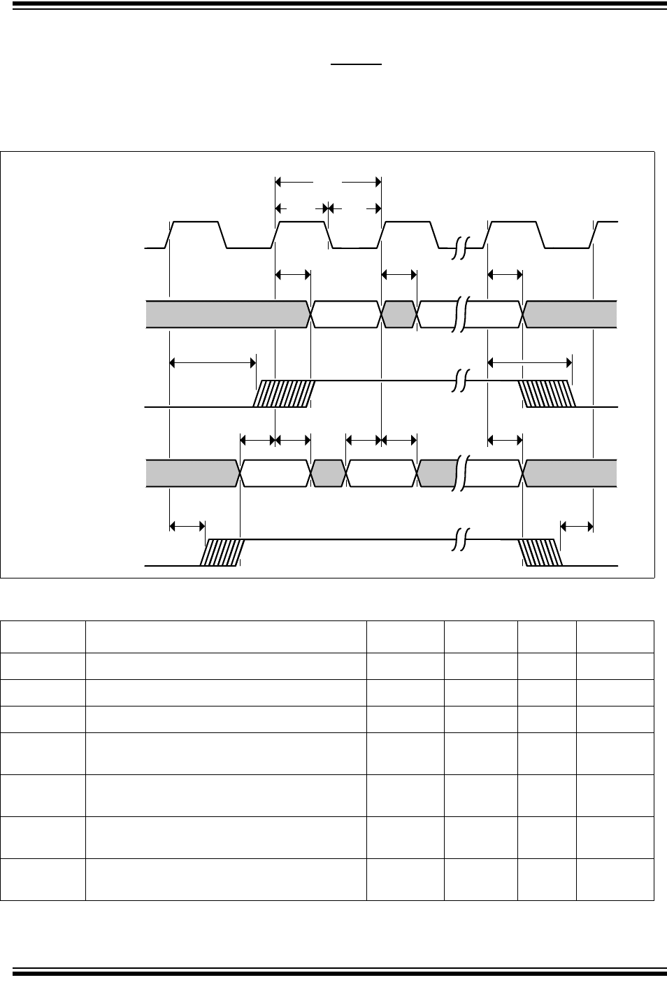
5.5.4.2 RMII Timing (REF_CLK In Mode)
The 50MHz REF_CLK IN timing applies to the case when nINTSEL is floated or pulled-high. In this mode, a 50MHz
clock must be input on the CLKIN pin. For more information on REF_CLK In Mode, see Section 3.7.4.1, REF_CLK In
Mode.
FIGURE 5-5: RMII TIMING (REF_CLK IN MODE)
CLKIN
(REF_CLK)
RXD[1:0],
RXER
CRS_DV
t
clkh
t
clkl
t
clkp
t
oval
t
ohold
t
oval
t
oval
t
ohold
t
su
TXD[1:0]
TXEN
t
ihold
t
su
t
ihold
t
ihold
t
su
t
ihold
TABLE 5-10: RMII TIMING VALUES (REF_CLK IN MODE)
Symbol Description Min Max Units Notes
t
clkp
CLKIN period 20 — ns —
t
clkh
CLKIN high time t
clkp
*0.35 t
clkp
*0.65 ns —
t
clkl
CLKIN low time t
clkp
*0.35 t
clkp
*0.65 ns —
t
oval
RXD[1:0], RXER, CRS_DV output valid from ris-
ing edge of CLKIN
— 14.0 ns Note 5-25
t
ohold
RXD[1:0], RXER, CRS_DV output hold from ris-
ing edge of CLKIN
3.0 — ns Note 5-25
t
su
TXD[1:0], TXEN setup time to rising edge of
CLKIN
4.0 — ns Note 5-25
t
ihold
TXD[1:0], TXEN input hold time after rising edge
of CLKIN
1.5 — ns Note 5-25
Note 5-25 T
iming was designed for system load between 10 pf and 25 pf.