
Datasheet
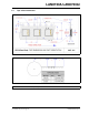
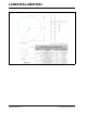
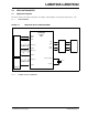
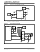
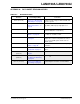
Table Of Contents
- Small Footprint RMII 10/100 Ethernet Transceiver with HP Auto-MDIX Support
- 1.0 Introduction
- 2.0 Pin Description and Configuration
- 3.0 Functional Description
- 3.1 Transceiver
- 3.2 Auto-negotiation
- 3.3 HP Auto-MDIX Support
- 3.4 MAC Interface
- 3.5 Serial Management Interface (SMI)
- 3.6 Interrupt Management
- 3.7 Configuration Straps
- 3.8 Miscellaneous Functions
- 3.9 Application Diagrams
- 4.0 Register Descriptions
- 4.1 Register Nomenclature
- 4.2 Control and Status Registers
- TABLE 4-2: SMI Register Map
- 4.2.1 Basic Control Register
- 4.2.2 Basic Status Register
- 4.2.3 PHY Identifier 1 Register
- 4.2.4 PHY Identifier 2 Register
- 4.2.5 Auto Negotiation Advertisement Register
- 4.2.6 Auto Negotiation Link Partner Ability Register
- 4.2.7 Auto Negotiation Expansion Register
- 4.2.8 Mode Control/Status Register
- 4.2.9 Special Modes Register
- 4.2.10 Symbol Error Counter Register
- 4.2.11 Special Control/Status Indications Register
- 4.2.12 Interrupt Source Flag Register
- 4.2.13 Interrupt Mask Register
- 4.2.14 PHY Special Control/Status Register
- 5.0 Operational Characteristics
- 6.0 Package Information
- 7.0 Application Notes
- Appendix A: Data Sheet Revision History
- The Microchip Web Site
- Customer Change Notification Service
- Customer Support
- Product Identification System
- Worldwide Sales and Service

2016 Microchip Technology Inc. DS00002165B-page 73
LAN8720A/LAN8720AI
APPENDIX A: DATA SHEET REVISION HISTORY
TABLE A-1: REVISION HISTORY
Revision Section/Figure/Entry Correction
Rev B. (07-15-16) Section 5.1, "Absolute Maxi-
mum Ratings*," on page 54
Update to Positive voltage on XTAL1/CLKIN, with
respe
ct to ground.
Table 5-2, “Non-Variable I/O
Buffer Characteristics,” on
page 56
Update to min/max values for the last row, ICLK
T
ype Buffer (XTAL1 Input) - High Input Level.
Rev. A (06-24-16) All Document converted to Microchip look and feel.
Rep
laces SMSC Rev. 1.4 (08-23-12).
Section 5.2, "Operating Con-
ditions**," on page 54
Increased VDDCR operational limits from “+1.14V
to
+1.26V” to “+1.08V to +1.32V”
Section 5.6, "Clock Circuit,"
on page 65
Added new 100uW crystal specifications and circuit
dia
gram. The section is now split into two subsec-
tions, one for 300uW crystals and the other for
100uW cryst
als.
Section 6.0, "Package Infor-
mation," on page 68
Added new subsections to include SQFN package
information.
Section , "Product Identifica-
tion System," on page 77
Updated ordering codes with sawn SQFN package
options.
Rev. 1.4
(08-23-12)
Section 4.2.2, Basic Status
Register
Updated definitions of bits 10:8.
Rev. 1.3
(04-20-11)
Table 5-9, “RMII Timing Val-
ues (REF_CLK Out Mode),”
on page 60
Updated t
oval
maximum value from 10.0ns to 5.0ns.
Rev. 1.2 (11-10-10) Section 5.5.5, "RMII Inter-
face Timing," on page 63
Updated diagrams and tables to include RXER.