
Datasheet


dsPIC33FJ16(GP/MC)101/102 AND dsPIC33FJ32(GP/MC)101/102/104
DS70000652F-page 150 2011-2014 Microchip Technology Inc.
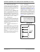
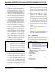
REGISTER 10-4: RPINR4: PERIPHERAL PIN SELECT INPUT REGISTER 4
U-0 U-0 U-0 R/W-1 R/W-1 R/W-1 R/W-1 R/W-1
— — —T5CKR4
(1)
T5CKR3
(1)
T5CKR2
(1)
T5CKR1
(1)
T5CKR0
(1)
bit 15 bit 8
U-0 U-0 U-0 R/W-1 R/W-1 R/W-1 R/W-1 R/W-1
— — —T4CKR4
(1)
T4CKR3
(1)
T4CKR2
(1)
T4CKR1
(1)
T4CKR0
(1)
bit 7 bit 0
Legend:
R = Readable bit W = Writable bit U = Unimplemented bit, read as ‘0’
-n = Value at POR ‘1’ = Bit is set ‘0’ = Bit is cleared x = Bit is unknown
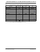
bit 15-13 Unimplemented: Read as ‘0’
bit 12-8 T5CKR<4:0>: Assign Timer5 External Clock (T5CK) to the Corresponding RPn Pin bits
(1)
11111 = Input tied to VSS
11110 = Reserved
.
.
.
11010 = Reserved
11001 = Input tied to RP25
.
.
.
00001 = Input tied to RP1
00000 = Input tied to RP0
bit 7-5 Unimplemented: Read as ‘0’
bit 4-0 T4CKR<4:0>: Assign Timer4 External Clock (T4CK) to the Corresponding RPn Pin bits
(1)
11111 = Input tied to VSS
11110 = Reserved
.
.
.
11010 = Reserved
11001 = Input tied to RP25
.
.
.
00001 = Input tied to RP1
00000 = Input tied to RP0
Note 1: These bits are available in dsPIC33FJ32(GP/MC)10X devices only.