
Datasheet

2011-2014 Microchip Technology Inc. DS70000652F-page 203
dsPIC33FJ16(GP/MC)101/102 AND dsPIC33FJ32(GP/MC)101/102/104
17.0 INTER-INTEGRATED CIRCUIT™
(I
2
C™)
The Inter-Integrated Circuit™ (I
2
C™) module provides
complete hardware support for both Slave and Multi-
Master modes of the I
2
C serial communication
standard, with a 16-bit interface.
The I
2
C module has a 2-pin interface:
• The SCLx pin is clock
• The SDAx pin is data
The I
2
C module offers the following key features:
•I
2
C interface supporting both Master and Slave
modes of operation
•I
2
C Slave mode supports 7-bit and 10-bit addresses
•I
2
C Master mode supports 7-bit and 10-bit addresses
•I
2
C port allows bidirectional transfers between
master and slaves
• Serial clock synchronization for I
2
C port can be
used as a handshake mechanism to suspend and
resume serial transfer (SCLREL control)
•I
2
C supports multi-master operation, detects bus
collision and arbitrates accordingly
17.1 Operating Modes
The hardware fully implements all the master and slave
functions of the I
2
C Standard and Fast mode
specifications, as well as 7-Bit and 10-Bit Addressing.
The I
2
C module can operate either as a slave or a
master on an I
2
C bus.
The following types of I
2
C operation are supported:
•I
2
C slave operation with 7-Bit Addressing
•I
2
C slave operation with 10-Bit Addressing
•I
2
C master operation with 7-Bit or
10-Bit Addressing
For details about the communication sequence in each
of these modes, refer to the Microchip web site
(www.microchip.com) for the latest “dsPIC33/PIC24
Family Reference Manual” sections.
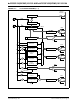
17.2 I
2
C Registers
I2CxCON and I2CxSTAT are control and status
registers, respectively. The I2CxCON register is
readable and writable. The lower six bits of I2CxSTAT
are read-only. The remaining bits of the I2CxSTAT are
read/write.
• I2CxRSR is the shift register used for shifting data
• I2CxRCV is the receive buffer and the register to
which data bytes are written or from which data
bytes are read
• I2CxTRN is the transmit register to which bytes
are written during a transmit operation
• I2CxADD register holds the slave address
• ADD10 status bit indicates 10-Bit Addressing
mode
• I2CxBRG acts as the Baud Rate Generator (BRG)
reload value
In receive operations, I2CxRSR and I2CxRCV together
form a double-buffered receiver. When I2CxRSR
receives a complete byte, it is transferred to I2CxRCV
and an interrupt pulse is generated.
Note 1: This data sheet summarizes the features
of the dsPIC33FJ16(GP/MC)101/102 and
dsPIC33FJ32(GP/MC)101/102/104 family
devices. It is not intended to be a
comprehensive reference source. To com-
plement the information in this data sheet,
refer to “Inter-Integrated Circuit™
(I
2
C™)” (DS70195) in the “dsPIC33/
PIC24 Family Reference Manual”, which
is available from the Microchip web site
(www.microchip.com).
2: Some registers and associated bits
described in this section may not be
available on all devices. Refer to
Section 4.0 “Memory Organization” in
this data sheet for device-specific register
and bit information.