
Datasheet


dsPIC33FJ16(GP/MC)101/102 AND dsPIC33FJ32(GP/MC)101/102/104
DS70000652F-page 262 2011-2014 Microchip Technology Inc.
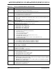
The Configuration Shadow register map is shown in Table 23-1.
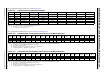
The Configuration Flash Word maps are shown in Table 23-2 and Table 23-3.
TABLE 23-2: CONFIGURATION FLASH WORDS FOR dsPIC33FJ16(GP/MC)10X DEVICES
(1)
TABLE 23-3: CONFIGURATION FLASH WORDS FOR dsPIC33FJ32(GP/MC)10X DEVICES
(1)
TABLE 23-1: CONFIGURATION SHADOW REGISTER MAP
File Name Addr. Bit 7 Bit 6 Bit 5 Bit 4 Bit 3 Bit 2 Bit 1 Bit 0
FGS F80004
— — — — — — GCP GWRP
FOSCSEL F80006 IESO PWMLOCK
(1)
— WDTWIN1 WDTWIN0 FNOSC2 FNOSC1 FNOSC0
FOSC F80008 FCKSM1 FCKSM0 IOL1WAY
— — OSCIOFNC POSCMD1 POSCMD0
FWDT F8000A FWDTEN WINDIS PLLKEN WDTPRE WDTPOST3 WDTPOST2 WDTPOST1 WDTPOST0
FPOR F8000C PWMPIN
(1)
HPOL
(1)
LPOL
(1)
ALTI2C1 — — — —
FICD F8000E Reserved
(2)
— Reserved
(3)
Reserved
(3)
— —ICS1ICS0
Legend: — = unimplemented, read as ‘1’.
Note 1: These bits are available in dsPIC33FJ(16/32)MC10X devices only.
2: This bit is reserved for use by development tools.
3: These bits are reserved, program as ‘0’.
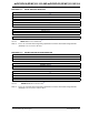
File
Name
Addr. Bits 23-16 Bit 15 Bit 14 Bit 13 Bit 12 Bit 11 Bit 10 Bit 9 Bit 8 Bit 7 Bit 6 Bit 5 Bit 4 Bit 3 Bit 2 Bit 1 Bit 0
CONFIG2 002BFC —IESOPWMLOCK
(2)
PWMPIN
(2)
WDTWIN1 WDTWIN0 FNOSC2 FNOSC1 FNOSC0 FCKSM1 FCKSM0 OSCIOFNC
(5)
IOL1WAY LPOL
(2)
ALTI2C1 POSCMD1 POSCMD0
CONFIG1 002BFE
—Reserved
(3)
Reserved
(3)
GCP GWRP Reserved
(4)
HPOL
(2)
ICS1 ICS0 FWDTEN WINDIS PLLKEN WDTPRE WDTPOST3 WDTPOST2 WDTPOST1 WDTPOST0
Legend:
— = unimplemented, read as ‘
1
’.
Note 1:
During a Power-on Reset (POR), the contents of these Flash locations are transferred to the Configuration Shadow registers.
2:
These bits are reserved in dsPIC33FJ16GP10X devices and read as ‘
1
’.
3:
These bits are reserved, program as ‘
0
’.
4:
This bit is reserved for use by development tools and must be programmed as ‘
1
’.
5:
This bit is programmed to ‘
0
’ during final tests in the factory.
File
Name
Addr. Bits 23-16 Bit 15 Bit 14 Bit 13 Bit 12 Bit 11 Bit 10 Bit 9 Bit 8 Bit 7 Bit 6 Bit 5 Bit 4 Bit 3 Bit 2 Bit 1 Bit 0
CONFIG2 0057FC — IESO PWMLOCK
(2)
PWMPIN
(2)
WDTWIN1 WDTWIN0 FNOSC2 FNOSC1 FNOSC0 FCKSM1 FCKSM0 OSCIOFNC
(5)
IOL1WAY LPOL
(2)
ALTI2C1 POSCMD1 POSCMD0
CONFIG1 0057FE
—Reserved
(3)
Reserved
(3)
GCP GWRP Reserved
(4)
HPOL
(2)
ICS1 ICS0 FWDTEN WINDIS PLLKEN WDTPRE WDTPOST3 WDTPOST2 WDTPOST1 WDTPOST0
Legend:
— = unimplemented, read as ‘
1
’.
Note 1:
During a Power-on Reset (POR), the contents of these Flash locations are transferred to the Configuration Shadow registers.
2:
These bits are reserved in dsPIC33FJ32GP10X devices and read as ‘
1
’.
3:
These bits are reserved, program as ‘
0
’.
4:
This bit is reserved for use by development tools and must be programmed as ‘
1
’.
5:
This bit is programmed to ‘
0
’ during final tests in the factory.