
Datasheet


2011-2014 Microchip Technology Inc. DS70000652F-page 335
dsPIC33FJ16(GP/MC)101/102 AND dsPIC33FJ32(GP/MC)101/102/104
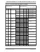
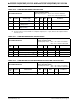
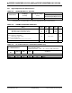
TABLE 26-49: 10-BIT ADC CONVERSION TIMING REQUIREMENTS
AC CHARACTERISTICS
Standard Operating Conditions: 3.0V to 3.6V
(unless otherwise stated)
Operating temperature -40°C T
A +85°C for Industrial
-40°C T
A +125°C for Extended
Param
No.
Symbol Characteristic Min. Typ
(1)
Max. Units Conditions
Clock Parameters
(2)
AD50 TAD ADC Clock Period 76 — — ns
AD51 tRC ADC Internal RC Oscillator Period — 250 — ns
Conversion Rates
AD55 t
CONV Conversion Time — 12 TAD ——
AD56 FCNV Throughput Rate — — 1.1 Msps
AD57 TSAMP Sample Time 2.0 TAD ———
Timing Parameters
AD60 t
PCS Conversion Start from Sample
Trigger
(1)
2.0 TAD — 3.0 TAD — Auto-Convert Trigger
(SSRC<2:0> = 111) not
selected
AD61 tPSS Sample Start from Setting
Sample (SAMP) bit
(1)
2.0 TAD — 3.0 TAD —
AD62 t
CSS Conversion Completion to
Sample Start (ASAM = 1)
(1)
—0.5 TAD ——
AD63 t
DPU Time to Stabilize Analog Stage
from ADC Off to ADC On
(1)
——20s
Note 1: These parameters are characterized but not tested in manufacturing.
2: Because the sample caps will eventually lose charge, clock rates below 10 kHz may affect linearity
performance, especially at elevated temperatures.