
Datasheet


2011-2014 Microchip Technology Inc. Preliminary DS70000652F-page 339
dsPIC33FJ16(GP/MC)101/102 AND dsPIC33FJ32(GP/MC)101/102/104
27.0 HIGH-TEMPERATURE ELECTRICAL CHARACTERISTICS
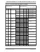
This section provides an overview of dsPIC33FJ16(GP/MC)101/102 and dsPIC33FJ32(GP/MC)101/102/104 family
electrical characteristics for devices operating in an ambient temperature range of -40°C to +150°C.
The specifications between -40°C to +150°C are identical to those shown in Section 26.0 “Electrical Characteristics”
for operation between -40°C to +125°C, with the exception of the parameters listed in this section.
Parameters in this section begin with an H, which denotes: High temperature. For example, Parameter DC10 in
Section 26.0 “Electrical Characteristics” is the Industrial and Extended temperature equivalent of HDC10.
Absolute maximum ratings for the dsPIC33FJ16(GP/MC)101/102 and dsPIC33FJ32(GP/MC)101/102/104 high-
temperature devices are listed below. Exposure to these maximum rating conditions for extended periods can affect
device reliability. Functional operation of the device at these or any other conditions, above the parameters indicated in
the operation listings of this specification, is not implied.
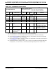
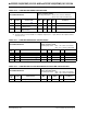
Absolute Maximum Ratings
(1)
Ambient temperature under bias
(3)
.........................................................................................................-40°C to +150°C
Storage temperature .............................................................................................................................. -65°C to +160°C
Voltage on VDD with respect to VSS ......................................................................................................... -0.3V to +4.0V
Voltage on any pin that is not 5V tolerant with respect to V
SS
(4)
.................................................... -0.3V to (VDD + 0.3V)
Voltage on any 5V tolerant pin with respect to VSS when VDD < 3.0V
(4)
....................................... -0.3V to (VDD + 0.3V)
Voltage on any 5V tolerant pin with respect to VSS when VDD 3.0V
(4)
.................................................... -0.3V to 5.6V
Maximum current out of V
SS pin ...........................................................................................................................300 mA
Maximum current into VDD pin
(2)
...........................................................................................................................250 mA
Maximum junction temperature.............................................................................................................................+155°C
Maximum current sourced/sunk by any 4x I/O pin....................................................................................................4 mA
Maximum current sourced/sunk by any 8x I/O pin....................................................................................................8 mA
Maximum current sunk by all ports combined ........................................................................................................80 mA
Maximum current sourced by all ports combined
(2)
................................................................................................80 mA
Note 1: Stresses above those listed under “Absolute Maximum Ratings” can cause permanent damage to the
device. This is a stress rating only and functional operation of the device at those, or any other conditions
above those indicated in the operation listings of this specification, is not implied. Exposure to maximum
rating conditions for extended periods can affect device reliability.
2: Maximum allowable current is a function of device maximum power dissipation (see Table 27-2).
3: AEC-Q100 reliability testing for devices intended to operate at +150°C is 1,000 hours. Any design in which
the total operating time from +125°C to +150°C will be greater than 1,000 hours is not warranted without
prior written approval from Microchip Technology Inc.
4: Refer to the “Pin Diagrams” section for 5V tolerant pins.