
Datasheet


dsPIC33FJ16(GP/MC)101/102 AND dsPIC33FJ32(GP/MC)101/102/104
DS70000652F-page 340 Preliminary 2011-2014 Microchip Technology Inc.
27.1 High-Temperature DC Characteristics
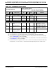
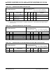
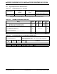
TABLE 27-1: OPERATING MIPS VS. VOLTAGE
TABLE 27-2: THERMAL OPERATING CONDITIONS
TABLE 27-3: DC CHARACTERISTICS: OPERATING CURRENT (I
DD))
Characteristic
V
DD Range
(in Volts)
Temperature Range
(in °C)
Max MIPS
dsPIC33FJ16(GP/MC)101/102 and
dsPIC33FJ32(GP/MC)101/102/104
HDC5 V
BOR – 3.6V
(1)
-40°C to +150°C 5
Note 1: Overall functional device operation at VBORMIN < VDD < VDDMIN is tested but not characterized. All device
analog modules, such as the ADC, etc., may have degraded performances below V
DDMIN.
Rating Symbol Min Typ Max Unit
High Temperature Devices
Operating Junction Temperature Range T
J -40 — +155 °C
Operating Ambient Temperature Range T
A -40 — +150 °C
Power Dissipation:
Internal chip power dissipation:
PINT = VDD x (IDD – IOH)
PD PINT + PI/O W
I/O Pin Power Dissipation:
I/O = ({V
DD – VOH} x IOH) + (VOL x IOL)
Maximum Allowed Power Dissipation PDMAX (TJ – TA)/JA W
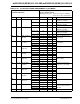
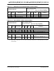
DC CHARACTERISTICS
Standard Operating Conditions: 3.0V to 3.6V
(unless otherwise stated)
Operating temperature -40°C TA +150°C for High Temperature
Parameter
No.
Typical Max Units Conditions
Operating Current (I
DD) – dsPIC33FJ16(GP/MC)10X Devices
DC20e 1.3 1.7 mA 3.3V LPRC (32.768 kHz)
DC22e 7.0 8.5 mA 3.3V 5 MIPS