
Datasheet


dsPIC33FJ16(GP/MC)101/102 AND dsPIC33FJ32(GP/MC)101/102/104
DS70000652F-page 66 2011-2014 Microchip Technology Inc.
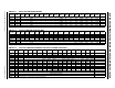
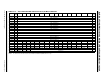
TABLE 4-18: CTMU REGISTER MAP
File Name
SFR
Addr
Bit 15 Bit 14 Bit 13 Bit 12 Bit 11 Bit 10 Bit 9 Bit 8 Bit 7 Bit 6 Bit 5 Bit 4 Bit 3 Bit 2 Bit 1 Bit 0
All
Resets
CTMUCON1 033A CTMUEN — CTMUSIDL TGEN EDGEN EDGSEQEN IDISSEN CTTRIG — — — — — — — —
0000
CTMUCON2 033C EDG1MOD EDG1POL EDG1SEL3 EDG1SEL2 EDG1SEL1 EDG1SEL0 EDG2STAT EDG1STAT EDG2MOD EDG2POL EDG2SEL3 EDG2SEL2 EDG2SEL1 EDG2SEL0 — —
0000
CTMUICON 033E ITRIM5 ITRIM4 ITRIM3 ITRIM2 ITRIM1 ITRIM0 IRNG1 IRNG0 — — — — — — — —
0000
Legend:
— = unimplemented, read as ‘
0
’. Reset values are shown in hexadecimal.
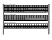
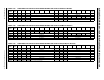
TABLE 4-19: REAL-TIME CLOCK AND CALENDAR REGISTER MAP
File Name
SFR
Addr
Bit 15 Bit 14 Bit 13 Bit 12 Bit 11 Bit 10 Bit 9 Bit 8 Bit 7 Bit 6 Bit 5 Bit 4 Bit 3 Bit 2 Bit 1 Bit 0
All
Resets
ALRMVAL 0620 Alarm Value Register Window based on ALRMPTR<1:0> xxxx
ALCFGRPT 0622 ALRMEN CHIME AMASK3 AMASK2 AMASK1 AMASK0
ALRMPTR1 ALRMPTR0
ARPT7 ARPT6 ARPT5 ARPT4 ARPT3 ARPT2 ARPT1 ARPT0 0000
RTCVAL 0624 RTCC Value Register Window based on RTCPTR<1:0> xxxx
RCFGCAL 0626 RTCEN
— RTCWREN RTCSYNC HALFSEC RTCOE RTCPTR1 RTCPTR0 CAL7 CAL6 CAL5 CAL4 CAL3 CAL2 CAL1 CAL0 0000
Legend: x = unknown value on Reset, — = unimplemented, read as ‘0’. Reset values are shown in hexadecimal.
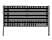
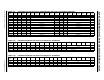
TABLE 4-20: PAD CONFIGURATION REGISTER MAP
File Name
SFR
Addr
Bit 15 Bit 14 Bit 13 Bit 12 Bit 11 Bit 10 Bit 9 Bit 8 Bit 7 Bit 6 Bit 5 Bit 4 Bit 3 Bit 2 Bit 1 Bit 0
All
Resets
PADCFG1 02FC
— — — — — — — — — — — — — — RTSECSEL — 0000
Legend: — = unimplemented, read as ‘0’. Reset values are shown in hexadecimal.