
Datasheet


MCP2200
DS22228B-page 6 2011 Microchip Technology Inc.
1.5.2.1 Internal Power Supply Details
MCP2200 offers various options for power supply. To
meet the required USB signaling levels, MCP2200
device incorporates an internal LDO used solely by the
USB transceiver, in order to present the correct D+/D-
voltage levels.
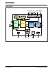
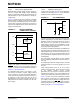
Figure 1-2 shows the internal connections of the USB
transceiver LDO in relation with the V
DD power supply
rail. The output of the USB transceiver LDO is tied to
the VUSB line. A capacitor connected to the VUSB pin is
required if the USB transceiver LDO provides the 3.3V
supply to the transceiver.
FIGURE 1-2: MCP2200 INTERNAL
POWER SUPPLY DETAILS
The provided VDD voltage has a direct influence on the
voltage levels present on the GPIO pins (Rx/Tx and
RTS
/CTS). When VDD is 5V, all of these pins will have
a logical ‘1’ around 5V with the variations specified in
Section 3.1, DC Characteristics.
For applications that require a 3.3V logical ‘1’ level,
V
DD must be connected to a power supply providing
the 3.3V voltage. In this case, the internal USB trans-
ceiver LDO cannot provide the required 3.3V power. It
is necessary to also connect the V
USB pin of the
MCP2200 to the 3.3V power supply rail. This way, the
USB transceiver is powered up directly from the 3.3V
power supply.
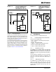
1.5.2.2 USB Bus Powered (5V)
In Bus Power Only mode, all power for the application
is drawn from the USB (Figure 1-3). This is effectively
the simplest power method for the device.
FIGURE 1-3: BUS POWER ONLY
In order to meet the inrush current requirements of the
USB 2.0 specifications, the total effective capacitance
appearing across V
BUS and ground must be no more
than 10 µF. If it is not more than 10 µF, some kind of
inrush limiting is required. For more details on Inrush
Current Limiting, search for that subject in the current
Universal Serial Bus Specification.
According to the USB 2.0 specification, all USB devices
must also support a Low-Power Suspend mode. In the
USB Suspend mode, devices must consume no more
than 500 µA (or 2.5 mA for high powered devices that
are remote wake-up capable) from the 5V V
BUS line of
the USB cable.
The host signals the USB device to enter Suspend
mode by stopping all USB traffic to that device for more
than 3 ms.
The USB bus provides a 5V voltage. However, the USB
transceiver requires 3.3V for the signaling (on D+ and
D- lines).
During USB Suspend mode, the D+ or D- pull-up
resistor must remain active, which will consume some
of the allowed suspend current budget
(500 µA/2.5 mA). The V
USB pin is required to have an
external bypass capacitor. It is recommended that the
capacitor be a ceramic cap, between 0.22 and 0.47 µF.
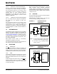
Figure 1-4 shows a circuit where MCP2200’s internal
LDO is used to provide 3.3V to the USB transceiver.
The voltage on the V
DD affects the voltage levels onto
the GPIO pins (Rx/Tx and RTS
/CTS). With VDD at 5V,
these pins will have a logic ‘1’ of 5V with the variations
specified in Section 3.1, DC Characteristics.
LDO
3.3V
USB
Transceiver
D+
V
DD
VUSB
D-
IN
OUT
VDD
VUSB
VSS
VBUS