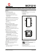
MCP2210 USB-to-SPI Protocol Converter with GPIO (Master Mode) Features: Package Types: Universal Serial Bus (USB) The device will be offered in the following packages: • 20-lead QFN (5 x 5 mm) • 20-lead SOIC • 20-lead SSOP MCP2210 SOIC, SSOP EEPROM • 256 Bytes of User EEPROM (accessible through certain USB commands) 2011 Microchip Technology Inc.
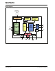
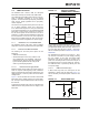
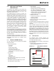
MCP2210 Block Diagram Dedicated function pins CS8:0 GP8-GP0 GPIO Chip Select Control SCK MISO MOSI USB Protocol Controller Control SPI (Master) USB XCVR 3.3V LDO Baud Generator State Clock VSS Vss DS22288A-page 2 Configuration and Control Regs 256-Byte EEPROM USB Clock OSC OSC1 OSC2 D+ D- VUSB Reset RST VDD 2011 Microchip Technology Inc.
MCP2210 1.0 FUNCTIONAL DESCRIPTION The MCP2210 also has 256 bytes of integrated user EEPROM. The MCP2210 device is a USB-to-SPI Master converter which enables USB connectivity in applications that have an SPI interface. The device reduces external components by integrating the USB termination resistors.
MCP2210 1.1 Supported Operating Systems The following operating systems are supported: • Windows XP/Vista/7 • Linux • Mac OS 1.1.1 1.3.2 SPI MODULE POWER-UP CONFIGURATION Default parameters: • 1 Mbit • 4 bytes to transfer per SPI transaction • GP1 as Chip Select line ENUMERATION The MCP2210 will enumerate as a USB device after Power-on Reset (POR). The device enumerates as a Human Interface Device (HID) only. 1.4 1.1.1.
MCP2210 1.5 USB Transceiver FIGURE 1-1: The MCP2210 has a built-in, USB 2.0, full-speed transceiver internally connected to the USB module. VDD The USB transceiver obtains power from the VUSB pin, which is internally connected to a 3.3V internal regulator. The best electrical signal quality is obtained when VUSB is locally bypassed with a high-quality ceramic capacitor. The internal 3.3V regulator draws power from the VDD pin. In certain scenarios, where VDD is lower than 3.
MCP2210 In order to meet the inrush current requirements of the USB 2.0 specifications, the total effective capacitance appearing across VBUS and ground must be no more than 10 µF. If it is more than 10 µF, some kind of inrush limiting is required. For more details on Inrush Current Limiting, see the current Universal Serial Bus Specification. According to the USB 2.0 specification, all USB devices must also support a Low-Power Suspend mode.
MCP2210 1.6 GP Module The GP module features nine I/O lines. 1.6.
MCP2210 1.7 EEPROM Module The EEPROM module is a 256-byte array of nonvolatile memory. The memory locations are accessed for read/write operations solely via USB host commands. The memory cells for data EEPROM are rated to endure thousands of erase/write cycles, up to 100K for EEPROM. 1.9 Oscillator The input clock must be 12 MHz to provide the proper frequency for the USB module. USB full-speed is nominally 12 Mb/s. The clock input accuracy is ±0.25% (2,500 ppm maximum).
MCP2210 2.0 MCP2210 FUNCTIONAL DESCRIPTION The MCP2210 uses NVRAM to store relevant chip settings. These settings are loaded by the chip during the power-up process and they are used for GP designation and SPI transfers. The NVRAM settings at power-up (or Reset) are loaded into the RAM portion of the chip and they can be altered through certain USB commands. This is very useful since it allows dynamic reconfiguring of the GPs or SPI transfer parameters.
MCP2210 • The delay between subsequent data bytes (Figure 2-2) FIGURE 2-2: DATA-TO-DATA DELAY TDATA2DATA CS SCK MOSI MISO • The delay between the end of the last byte (of the SPI transfer) and the de-assertion of the Chip Select(s) FIGURE 2-3: DATA TO CHIP SELECT DELAY TDATA2CS CS SCK MOSI MISO For a particular SPI transfer, the user can choose any number (out of the available ones) of Chip Select pins.
MCP2210 3.
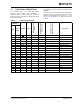
MCP2210 TABLE 3-1: COMMAND STRUCTURE (CONTINUED) Byte Index Meaning 9 GP5 Pin Designation • GPIO = 0x00 • Chip Selects = 0x01 • Dedicated Function pin = 0x02 10 GP6 Pin Designation • GPIO = 0x00 • Chip Selects = 0x01 • Dedicated Function pin = 0x02 11 GP7 Pin Designation • GPIO = 0x00 • Chip Selects = 0x01 • Dedicated Function pin = 0x02 12 GP8 Pin Designation • GPIO = 0x00 • Chip Selects = 0x01 • Dedicated Function pin = 0x02 13 Default GPIO Output – 16-bit value (low byte): • MSB – – – – – –
MCP2210 TABLE 3-1: COMMAND STRUCTURE (CONTINUED) Byte Index Meaning 17 Other Chip Settings – Enable/Disable Wake-up, Interrupt Counting, SPI Bus Release Options • Bit 7 – Don’t Care • Bit 6 – Don’t Care • Bit 5 – Don’t Care • Bit 4 – Remote Wake-up Enabled/Disabled - 0 – Remote Wake-up Disabled - 1 – Remote Wake-up Enabled • Bit 3 – Dedicated Function – Interrupt Pin mode • Bit 2 – Dedicated Function – Interrupt Pin mode • Bit 1 – Dedicated Function – Interrupt Pin mode - b111 – Reserved - b110 – Reser
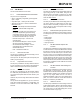
MCP2210 TABLE 3-3: RESPONSE 2 STRUCTURE Byte Index 0 Meaning 0x60 – Set Chip NVRAM Parameters – echos back the given command code 1 0x00 – Command Completed Successfully – settings written 2 0x20 – Sub-command Echoed Back for Set Chip Settings Power-up Default code 3-63 Don’t Care FIGURE 3-1: SET CHIP SETTINGS POWER-UP DEFAULT LOGIC FLOW Set NVRAM Chip Settings FALSE Conditional Access TRUE TRUE TRUE Response 2 DS22288A-page 14 Password Protected FALSE Was access FALSE password previous
MCP2210 3.1.
MCP2210 TABLE 3-4: COMMAND STRUCTURE (CONTINUED) Byte Index Meaning 17 Delay Between Subsequent Data Bytes (quanta of 100 µs) – 16-bit value (high byte) Example: If 500 µs delay between two consecutive data bytes is required, the value will be 0x0005. - Fill this byte position with: 0x00 18 Bytes to Transfer per SPI Transaction – 16-bit value (low byte) Example: If an SPI transaction of 1250 bytes long is required, the corresponding hex value will be 0x04E2.
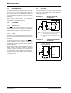
MCP2210 FIGURE 3-2: SET SPI POWER-UP TRANSFER SETTINGS LOGIC FLOW Set NVRAM SPI Transfers Settings FALSE SPI Transfer Ongoing TRUE Response 2 FALSE Conditional Access TRUE Requested NVRAM SPI Settings Not Written TRUE TRUE Password Protected Was access FALSE password previously entered correctly? FALSE Response 1 Requested NVRAM SPI Settings Not Written Permanent Lock Response 1 Response 3 Requested NVRAM SPI Settings Not Written Wrong Password 2011 Microchip Technology Inc.
MCP2210 3.1.
MCP2210 FIGURE 3-3: SET USB POWER-UP KEY PARAMETERS LOGIC FLOW Set NVRAM USB Key Parameters FALSE TRUE Conditional Access TRUE TRUE Response 2 2011 Microchip Technology Inc.
MCP2210 3.1.4 SET USB MANUFACTURER NAME TABLE 3-11: COMMAND STRUCTURE Byte Index Meaning 0 0x60 – Set Chip NVRAM Parameters – command code 1 0x50 – Set USB Manufacturer Name – sub-command code 2 0x00 – Reserved 3 0x00 – Reserved 4 Total USB String Descriptor Length (this is the length of the Manufacturer string, multiplied by 2 + 2) Example: “Microchip Technology Inc.” has 25 Unicode characters.
MCP2210 FIGURE 3-4: SET USB MANUFACTURER LOGIC FLOW Set NVRAM USB Manufacturer Name FALSE Conditional Access TRUE TRUE TRUE Response 1 2011 Microchip Technology Inc.
MCP2210 3.1.5 SET USB PRODUCT NAME TABLE 3-14: COMMAND STRUCTURE Byte Index Meaning 0 0x60 – Set Chip NVRAM Parameters – command code 1 0x40 – Set USB Product Name – sub-command code 2 0x00 – Reserved 3 0x00 – Reserved 4 Total USB String Descriptor Length (this is the length of the Product string multiplied by 2 + 2) Example: “MCP2210 USB to SPI Master” has 25 Unicode characters.
MCP2210 FIGURE 3-5: SET USB PRODUCT NAME LOGIC FLOW Set NVRAM USB Product Name FALSE Conditional Access TRUE TRUE TRUE Response 2 2011 Microchip Technology Inc.
MCP2210 3.1.6 GET SPI POWER-UP TRANSFER SETTINGS TABLE 3-17: COMMAND STRUCTURE Byte Index 0 Meaning 0x61 – Get NVRAM Settings – command code 1 0x10 – Get SPI Power-up Transfer Settings – sub-command code 2 0x00 – Reserved 3-63 0x00 – Reserved 3.1.6.
MCP2210 TABLE 3-18: RESPONSE 1 STRUCTURE (CONTINUED) Byte Index Meaning 14 Last Data Byte to CS (De-asserted) Delay (quanta of 100 µs) – 16-bit value (low byte) Example: If a 500 µs delay between the last data byte sent and the CS being de-asserted is required, the value will be 0x0005.
MCP2210 3.1.7 GET POWER-UP CHIP SETTINGS TABLE 3-19: COMMAND STRUCTURE Byte Index 0 Meaning 0x61 – Get NVRAM Settings – command code 1 0x20 – Get Power-up Chip Settings – sub-command code 2 0x00 – Reserved 3-63 0x00 – Reserved 3.1.7.
MCP2210 TABLE 3-20: RESPONSE 1 STRUCTURE (CONTINUED) Byte Index Meaning 11 GP7 Pin Designation • GPIO = 0x00 • Chip Selects = 0x01 • Dedicated Function pin = 0x02 12 GP8 Pin Designation • GPIO = 0x00 • Chip Selects = 0x01 • Dedicated Function pin = 0x02 13 Default GPIO Output – 16-bit value (low byte): • MSB – – – – – – LSB GP7 GP6 GP5 GP4 GP3 GP2 GP1 GP0 14 Default GPIO Output – 16-bit value (high byte): • MSB – – – – – – LSB x x x x x x x GP8 where x = Don’t Care 15 Default GPIO Direction – 1
MCP2210 FIGURE 3-7: GET POWER-UP CHIP SETTINGS LOGIC FLOW Get NVRAM Chip Settings Response 1 NVRAM Chip Settings Retrieved DS22288A-page 28 2011 Microchip Technology Inc.
MCP2210 3.1.8 GET USB KEY PARAMETERS TABLE 3-21: COMMAND STRUCTURE Byte Index Meaning 0 0x61 – Get NVRAM Settings – command code 1 0x30 – Get USB Key Parameters – sub-command code 2 0x00 – Reserved 3-63 0x00 – Reserved 3.1.8.
MCP2210 3.1.9 GET USB MANUFACTURER NAME TABLE 3-23: COMMAND STRUCTURE Byte Index 0 Meaning 0x61 – Get NVRAM Settings – command code 1 0x50 – Get USB Manufacturer Name – sub-command code 2 0x00 – Reserved 3-63 0x00 – Reserved 3.1.9.
MCP2210 3.1.10 GET USB PRODUCT NAME TABLE 3-25: COMMAND STRUCTURE Byte Index Meaning 0 0x61 – Get NVRAM Settings – command code 1 0x40 – Get USB Product Name – sub-command code 2 0x00 – Reserved 3-63 0x00 – Reserved 3.1.10.
MCP2210 3.1.11 SEND ACCESS PASSWORD TABLE 3-27: COMMAND STRUCTURE Byte Index Meaning 0 0x70 – SEND ACCESS Password – command code 1 0x00 – Reserved 2 0x00 – Reserved 3 0x00 – Reserved 4 Password Character 0 5 Password Character 1 6 Password Character 2 7 Password Character 3 8 Password Character 4 9 Password Character 5 10 Password Character 6 11 Password Character 7 12-63 3.1.11.
MCP2210 TABLE 3-31: RESPONSE 4 STRUCTURE Byte Index Meaning 0 0x70 – SEND ACCESS Password – echos back the given command code 1 0xFB – Access Not Allowed – Chip conditional access is on, the password does not match and the number of attempts is above the accepted threshold of 5. The Access Password mechanism is temporarily blocked and no further password access will be accepted until the next power-up.
MCP2210 3.2 Read/Write RAM Settings The set of commands/responses described in this section relates to the manipulation of the RAM settings (volatile). 3.2.1 GET (VM) SPI TRANSFER SETTINGS TABLE 3-33: COMMAND STRUCTURE Byte Index Meaning 0 0x41 – Get (VM) SPI Transfer Settings – command code 1 0x00 – Reserved 2 0x00 – Reserved 3-63 0x00 – Reserved 3.2.1.
MCP2210 TABLE 3-34: RESPONSE 1 STRUCTURE Byte Index Meaning 13 Chip Select to Data Delay (quanta of 100 µs) – 16-bit value (high byte) Example: If we have 500 µs delay between the CS being asserted and the first byte of data, the value will be 0x0005.
MCP2210 3.2.
MCP2210 TABLE 3-35: COMMAND 1 STRUCTURE (CONTINUED) Byte Index Meaning 16 Delay Between Subsequent Data Bytes (quanta of 100 µs) – 16-bit value (low byte) Example: If a 500 µs delay between two consecutive data bytes is required, the value will be 0x0005. - This byte position will have a value of: 0x05 17 Delay Between Subsequent Data Bytes (quanta of 100 µs) – 16-bit value (high byte) Example: If a 500 µs delay between two consecutive data bytes is required, the value will be 0x0005.
MCP2210 TABLE 3-36: RESPONSE 1 STRUCTURE (CONTINUED) Byte Index Meaning 10 Active Chip Select Value – 16-bit value (low byte): • MSB – – – – – – LSB CS7 CS6 CS5 CS4 CS3 CS2 CS1 CS0 11 Active Chip Select Value – 16-bit value (high byte): • MSB – – – – – – LSB x x x x x x x CS8 12 Chip Select to Data Delay (quanta of 100 µs) – 16-bit value (low byte) Example: If we have 500 µs delay between the CS being asserted and the first byte of data, the value will be 0x0005.
MCP2210 TABLE 3-37: RESPONSE 2 STRUCTURE Byte Index Meaning 0 0x40 – Set (VM) SPI Transfer Settings – echos back the given command code 1 0xF8 – USB transfer in progress – Settings not written 2 Don’t Care 3-63 Don’t Care FIGURE 3-13: SET (VM) SPI TRANSFER SETTINGS LOGIC FLOW Set RAM SPI Transfer Settings FALSE SPI Transfer Ongoing Response 1 TRUE Response 2 Requested RAM SPI Settings Not Written 3.2.
MCP2210 3.2.3.
MCP2210 TABLE 3-39: RESPONSE 1 STRUCTURE (CONTINUED) Byte Index 14 Meaning Default GPIO Output – 16-bit value (high byte): • MSB – – – – – – LSB x x x x x x x GP8 where x = Don’t Care 15 Default GPIO Direction – 16-bit value (low byte): • MSB – – – – – – LSB GP7DIR GP6DIR GP5DIR GP4DIR GP3DIR GP2DIR GP1DIR GP0DIR 16 Default GPIO Direction – 16-bit value (high byte): • MSB – – – – – – LSB x x x x x x x GP8DIR 17 Other Chip Settings – Enable/Disable Wake-up, Interrupt Counting, SPI Bus Release Option
MCP2210 FIGURE 3-14: GET (VM) CURRENT CHIP SETTINGS LOGIC FLOW Get RAM Chip Settings Response 1 RAM Chip Settings Retrieved 3.2.
MCP2210 TABLE 3-40: COMMAND STRUCTURE (CONTINUED) Byte Index Meaning 9 GP5 Pin Designation • GPIO = 0x00 • Chip Selects = 0x01 • Dedicated Function pin = 0x02 10 GP6 Pin Designation • GPIO = 0x00 • Chip Selects = 0x01 • Dedicated Function pin = 0x02 11 GP7 Pin Designation • GPIO = 0x00 • Chip Selects = 0x01 • Dedicated Function pin = 0x02 12 GP8 Pin Designation • GPIO = 0x00 • Chip Selects = 0x01 • Dedicated Function pin = 0x02 13 Default GPIO Output – 16-bit value (low byte): • MSB – – – – – –
MCP2210 TABLE 3-40: COMMAND STRUCTURE (CONTINUED) Byte Index 17 18-63 Meaning Other Chip Settings – Enable/Disable Wake-up, Interrupt Counting, SPI Bus Release Options • Bit 7 – Don’t Care • Bit 6 – Don’t Care • Bit 5 – Don’t Care • Bit 4 – Remote Wake-up Enabled/Disabled - 0 – Remote Wake-up Disabled - 1 – Remote Wake-up Enabled • Bit 3 – Dedicated Function – Interrupt Pin mode • Bit 2 – Dedicated Function – Interrupt Pin mode • Bit 1 – Dedicated Function – Interrupt Pin mode - b111 – Reserved - b110 –
MCP2210 TABLE 3-41: RESPONSE 1 STRUCTURE Byte Index Meaning 0 0x21 – Set (VM) Current Chip Settings – echos back the given command code 1 0x00 – Command Completed Successfully 2 Don’t Care 3-63 Don’t Care FIGURE 3-15: SET (VM) CURRENT CHIP SETTINGS LOGIC FLOW Set RAM Chip Settings Response 1 RAM Chip Settings Written 2011 Microchip Technology Inc.
MCP2210 3.2.5 GET (VM) GPIO CURRENT PIN DIRECTION TABLE 3-42: COMMAND STRUCTURE Byte Index Meaning 0 0x33 – Get (VM) GPIO Current Pin Direction 1 0x00 – Reserved 2 0x00 – Reserved 3-63 0x00 – Reserved 3.2.5.
MCP2210 3.2.6 SET (VM) GPIO CURRENT PIN DIRECTION TABLE 3-44: COMMAND STRUCTURE Byte Index Meaning 0 0x32 – Set (VM) GPIO Current Pin Direction 1 0x00 – Reserved 2 0x00 – Reserved 3 0x00 – Reserved 4 GPIO Direction – 16-bit value (low byte): • MSB – – – – – – LSB GP7DIR GP6DIR GP5DIR GP4DIR GP3DIR GP2DIR GP1DIR GP0DIR 5 GPIO Direction – 16-bit value (high byte): • MSB – – – – – – x x x x x x x 6-63 3.2.6.
MCP2210 3.2.7 GET GPIO CURRENT PIN VALUE TABLE 3-46: COMMAND STRUCTURE Byte Index Meaning 0 0x31 – Get (VM) GPIO Current Pin Value 1 0x00 – Reserved 2 0x00 – Reserved 3-63 0x00 – Reserved 3.2.7.
MCP2210 3.2.8 SET GPIO CURRENT PIN VALUE TABLE 3-48: COMMAND STRUCTURE Byte Index Meaning 0 0x30 – Set (VM) GPIO Current Pin Value 1 0x00 – Reserved 2 0x00 – Reserved 3 0x00 – Reserved 4 GPIO Pin Value – 16-bit value (low byte): • MSB – – – – – – LSB GP7VAL GP6VAL GP5VAL GP4VAL GP3VAL GP2VAL GP1VAL GP0VAL 5 GPIO Pin Value – 16-bit value (high byte): • MSB – – – – – – x x x x x x x 6-63 Note 1: 3.2.8.
MCP2210 3.3 Read/Write EEPROM Memory This set of commands/responses described in this section relates to the manipulation of the EEPROM memory. 3.3.1 READ EEPROM MEMORY TABLE 3-50: COMMAND STRUCTURE Byte Index Meaning 0 0x50 – READ EEPROM Memory – command code 1 EEPROM Memory Address to be read 2 0x00 – Reserved 3-63 0x00 – Reserved 3.3.1.
MCP2210 3.3.2 WRITE EEPROM MEMORY TABLE 3-52: COMMAND STRUCTURE Byte Index 0 Meaning 0x51 – WRITE EEPROM Memory – command code 1 EEPROM Memory Address to be written 2 The value to be written to at the given address 3-63 3.3.2.
MCP2210 FIGURE 3-21: WRITE EEPROM MEMORY LOGIC FLOW Write EEPROM Memory Location FALSE Conditional Access TRUE TRUE FALSE Password Protected Permanent Lock Response 3 TRUE Was access password previously FALSE entered correctly? Requested EEPROM Memory Location Not Written Wrong Password FALSE EEPROM Write Failure TRUE Response 1 Response 2 EEPROM Memory Location Written Requested NVRAM SPI Settings Not Written DS22288A-page 52 Response 3 Requested EEPROM Memory Location Not Written 20
MCP2210 3.4 External Interrupt Pin (GP6) Event Status The External Interrupt pin event status command is used by the USB host to query the external interrupt events recorded by the MCP2210. In order to have the MCP2210 record the number of external interrupt events, GP6 must be configured to have its dedicated function active. 3.4.
MCP2210 3.5 SPI Data Transfer The set of commands/responses described in this section relates to the SPI data transfer functionality. 3.5.1 TRANSFER SPI DATA TABLE 3-58: COMMAND STRUCTURE Byte Index Meaning 0 0x42 – Transfer SPI Data – command code 1 The number of bytes to be transferred in this packet (from 0 to 60 inclusively) 2 0x00 – Reserved 3 0x00 – Reserved 4-63 3.5.1.
MCP2210 TABLE 3-62: RESPONSE 4 STRUCTURE Byte Index Meaning 0 0x42 – Transfer SPI Data – echos back the given command code 1 0x00 – SPI Data accepted – Command Completed Successfully – SPI data accepted 2 How many SPI received data bytes the chip is sending back to the host 3 0x30 – SPI Transfer Engine Status: SPI transfer not finished; received data available 4-63 TABLE 3-63: SPI received data bytes.
MCP2210 3.5.2 CANCEL THE CURRENT SPI TRANSFER TABLE 3-64: COMMAND STRUCTURE Byte Index Meaning 0 0x11 – CANCEL the current SPI transfer – command code 1 0x00 – Reserved 2 0x00 – Reserved 3-63 0x00 – Reserved 3.5.2.
MCP2210 3.5.3 REQUEST SPI BUS RELEASE TABLE 3-66: COMMAND STRUCTURE Byte Index Meaning 0 0x80 – Request SPI bus Release – command code 1 The value of the SPI Bus Release ACK pin (only if GP7 is assigned to this dedicated function) 2 0x00 – Reserved 3-63 0x00 – Reserved 3.5.3.
MCP2210 FIGURE 3-25: REQUEST SPI BUS RELEASE LOGIC FLOW Request SPI Bus Release TRUE SPI Transfer Ongoing Response 2 SPI Bus Release Not Accepted SPI Transfer Ongoing DS22288A-page 58 FALSE Response 1 SPI Bus Release Accepted 2011 Microchip Technology Inc.
MCP2210 3.6 Chip Status The chip status command is used to retrieve status information regarding the state of the SPI transfer engine. 3.6.1 GET MCP2210 STATUS TABLE 3-69: COMMAND STRUCTURE Byte Index Meaning 0 0x10 – Get MCP2210 Status – command code 1 0x00 – Reserved 2 0x00 – Reserved 3-63 0x00 – Reserved 3.6.1.
MCP2210 3.6.2 UNSUPPORTED COMMAND CODES TABLE 3-71: COMMAND STRUCTURE Byte Index Meaning 0 Usupported Command Code 1 Don’t Care 2-63 Don’t Care 3.6.2.1 Responses TABLE 3-72: RESPONSE 1 STRUCTURE Byte Index Meaning 0 Unsupported Command Code Sent – echos back the given command code 1 0xF9 – Unknown Command – No effect 2-63 Don’t Care DS22288A-page 60 2011 Microchip Technology Inc.
MCP2210 NOTES: 2011 Microchip Technology Inc.
MCP2210 4.0 ELECTRICAL CHARACTERISTICS Absolute Maximum Ratings (†) Ambient temperature under bias ......................................................................................................... -40°C to +85°C Storage temperature ........................................................................................................................ -65°C to +150°C Voltage on VDD with respect to VSS ..................................................................................................
MCP2210 4.1 DC CHARACTERISTICS DC Characteristics Param No. D001 Characteristic Operating Conditions (unless otherwise indicated): 3.0V VDD 5.5V at -40C TA +85C (I-Temp) Sym Min Typ Max Units Supply Voltage VDD 3.3 — 5.5 V Power-on Reset Release Voltage VPOR Power-on Reset Rearm Voltage D003 VDD Rise Rate to Ensure Power-on Reset D004 Supply Current V 0.8 V 0.05 — — VDD = 3.0V — 10 12 mA VDD = 5.0V — 13 15 mA — 9 — µA — — 0.
MCP2210 FIGURE 4-1: POR AND POR REARM WITH SLOW RISING VDD VDD VPOR VPORR VSS NPOR(1) POR REARM VSS TPOR(3) TVLOW(2) Note 1: 2: 3: TABLE 4-1: USB MODULE SPECIFICATIONS DC Characteristics Param No. When NPOR is low, the device is held in Reset. TPOR 1 s typical. TVLOW 2.7 s typical. Characteristic Operating Conditions (unless otherwise indicated): 3.0V VDD 5.5V at -40C TA +85C (I-Temp) Sym Min Typ Max Units Conditions VUSB 3.0 — 3.
MCP2210 TABLE 4-2: THERMAL CONSIDERATIONS Standard Operating Conditions (unless otherwise stated) Operating temperature -40C TA +85C (I-Temp) Param No. Sym TH01 θJA Thermal Resistance Junction to Ambient TH02 θJC Thermal Resistance Junction to Case TH03 TH04 TJMAX PD Maximum Junction Temperature Power Dissipation TH05 TH06 TH07 Note 1: 2: 3: Characteristic PINTERNAL Internal Power Dissipation PI/O I/O Power Dissipation Typ Units 85.2 108.1 36.1 24 24 1.
MCP2210 4.2 AC Characteristics 4.2.1 TIMING PARAMETER SYMBOLOGY The timing parameter symbols have been created in one of the following formats: 1. TppS2ppS T F Frequency E Error Lowercase letters (pp) and their meanings: pp io Input or Output pin rx Receive bitclk RX/TX BITCLK drt Device Reset Timer Uppercase letters and their meanings: S F Fall H High I Invalid (high-impedance) L Low 4.2.2 2.
MCP2210 4.2.3 TIMING DIAGRAMS AND SPECIFICATIONS TABLE 4-4: RESET, OSCILLATOR START-UP TIMER AND POWER-UP TIMER PARAMETERS Standard Operating Conditions (unless otherwise stated) Operating Temperature -40°C TA +85°C Param No. Sym 30 TRST 31 32 Characteristic MCLR Pulse Width (low) TPWRT Power-up timer TOST Oscillator start-up time Min Typ† Max Units 2 — — μs 40 65 140 ms — 1024 — TOST Conditions * These parameters are characterized but not tested.
MCP2210 5.0 PACKAGING INFORMATION 5.1 Package Marking Information 20-Lead 5x5 QFN PIN 1 Example PIN 1 20-Lead SOIC MCP2210 I/MQ ^^ e3 1146256 Example MCP2210 I/SO ^^ e3 1146256 20-Lead SSOP Example MCP2210 I/SS ^^ e3 1146256 Legend: XX...
MCP2210 20-Lead Plastic Quad Flat, No Lead Package (MQ) 5x5x0.9 mm Body [QFN] Note: For the most current package drawings, please see the Microchip Packaging Specification located at http://www.microchip.com/packaging Microchip Technology Drawing C04-120A 2011 Microchip Technology Inc.
MCP2210 Note: For the most current package drawings, please see the Microchip Packaging Specification located at http://www.microchip.com/packaging DS22288A-page 70 2011 Microchip Technology Inc.
MCP2210 Note: For the most current package drawings, please see the Microchip Packaging Specification located at http://www.microchip.com/packaging 2011 Microchip Technology Inc.
MCP2210 Note: For the most current package drawings, please see the Microchip Packaging Specification located at http://www.microchip.com/packaging DS22288A-page 72 2011 Microchip Technology Inc.
MCP2210 Note: For the most current package drawings, please see the Microchip Packaging Specification located at http://www.microchip.com/packaging 2011 Microchip Technology Inc.
MCP2210 /HDG 3ODVWLF 6KULQN 6PDOO 2XWOLQH 66 ± PP %RG\ >6623@ 1RWH )RU WKH PRVW FXUUHQW SDFNDJH GUDZLQJV SOHDVH VHH WKH 0LFURFKLS 3DFNDJLQJ 6SHFLILFDWLRQ ORFDWHG DW KWWS ZZZ PLFURFKLS FRP SDFNDJLQJ D N E E1 NOTE 1 1 2 e b c A2 A φ A1 L1 8QLWV 'LPHQVLRQ /LPLWV 1XPEHU RI 3LQV L 0,//,0(7(56 0,1 1 120 0$; 3LWFK H 2YHUDOO +HLJKW $ ± %6& ± 0ROGHG 3DFNDJH 7KLFNQHVV $ 6WDQGRII $ ± ± 2YHUDOO :LGWK ( 0ROGHG 3DFNDJH
MCP2210 Note: For the most current package drawings, please see the Microchip Packaging Specification located at http://www.microchip.com/packaging 2011 Microchip Technology Inc.
MCP2210 NOTES: DS22288A-page 76 2011 Microchip Technology Inc.
MCP2210 APPENDIX A: REVISION HISTORY Revision A (December, 2011) • Original Release of this Document. 2011 Microchip Technology Inc.
MCP2210 NOTES: DS22288A-page 78 2011 Microchip Technology Inc.
MCP2210 PRODUCT IDENTIFICATION SYSTEM To order or obtain information, e.g., on pricing or delivery, refer to the factory or the listed sales office. PART NO. X /XX Device Temperature Range Package Device: MCP2210: MCP2210T: Examples: a) USB to SPI Protocol Converter with GPIO USB to SPI Protocol Converter with GPIO (Tape and Reel) Temperature Range: I = Package: MQ = Plastic Quad Flat, No Lead Package 5x5x0.9 mm Body (QFN), 20-Lead = Plastic Small Outline - Wide, 7.
MCP2210 NOTES: DS22288A-page 80 2011 Microchip Technology Inc.
Note the following details of the code protection feature on Microchip devices: • Microchip products meet the specification contained in their particular Microchip Data Sheet. • Microchip believes that its family of products is one of the most secure families of its kind on the market today, when used in the intended manner and under normal conditions. • There are dishonest and possibly illegal methods used to breach the code protection feature.
Worldwide Sales and Service AMERICAS ASIA/PACIFIC ASIA/PACIFIC EUROPE Corporate Office 2355 West Chandler Blvd. Chandler, AZ 85224-6199 Tel: 480-792-7200 Fax: 480-792-7277 Technical Support: http://www.microchip.com/ support Web Address: www.microchip.