
Datasheet


© 2007 Microchip Technology Inc. DS21919E-page 19
MCP23008/MCP23S08
1.6.10 PORT (GPIO) REGISTER
The GPIO register reflects the value on the port.
Reading from this register reads the port. Writing to this
register modifies the Output Latch (OLAT) register.
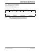
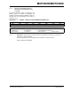
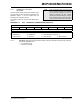
REGISTER 1-10: GPIO – GENERAL PURPOSE I/O PORT REGISTER (ADDR 0x09)
R/W-0 R/W-0 R/W-0 R/W-0 R/W-0 R/W-0 R/W-0 R/W-0
GP7 GP6 GP5 GP4 GP3 GP2 GP1 GP0
bit 7 bit 0
Legend:
R = Readable bit W = Writable bit U = Unimplemented bit, read as ‘0’
-n = Value at POR ‘1’ = Bit is set ‘0’ = Bit is cleared x = Bit is unknown
bit 7-0 GP7:GP0: These bits reflect the logic level on the pins <7:0>
1 = Logic-high.
0 = Logic-low.