MCP23008/MCP23S08 8-Bit I/O Expander with Serial Interface Features • 8-bit remote bidirectional I/O port - I/O pins default to input • High-speed I2C™ interface (MCP23008) - 100 kHz - 400 kHz - 1.
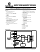
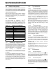
MCP23008/MCP23S08 Package Types MCP23008 1 2 3 4 5 6 7 8 9 18 17 16 15 14 13 12 11 10 SSOP SCL SDA A2 A1 A0 RESET NC INT VSS N/C VDD GP7 GP6 GP5 GP4 GP3 GP2 GP1 GP0 1 2 3 4 5 6 7 8 9 10 MCP23008 SCL SDA A2 A1 A0 RESET NC INT VSS MCP23008 PDIP/SOIC 20 19 18 17 16 15 14 13 12 11 VDD GP7 GP6 GP5 GP4 GP3 GP2 GP1 GP0 N/C DS21919E-page 2 SDA SCL VDD VSS GP7 20 19 18 17 16 QFN A2 1 15 GP6 A1 2 14 GP5 A0 3 13 GP4 RESET 4 12 GP3 NC 5 11 GP2 6 7 8 9 10 N/C INT N/C G
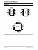
MCP23008/MCP23S08 Package Types: (Continued) MCP23S08 1 2 3 4 5 6 7 8 9 18 17 16 15 14 13 12 11 10 SSOP SCK SI SO A1 A0 RESET CS INT VSS N/C VDD GP7 GP6 GP5 GP4 GP3 GP2 GP1 GP0 1 2 3 4 5 6 7 8 9 10 MCP23S08 SCK SI SO A1 A0 RESET CS INT VSS MCP23S08 PDIP/SOIC 20 19 18 17 16 15 14 13 12 11 VDD GP7 GP6 GP5 GP4 GP3 GP2 GP1 GP0 N/C © 2007 Microchip Technology Inc.
MCP23008/MCP23S08 NOTES: DS21919E-page 4 © 2007 Microchip Technology Inc.
MCP23008/MCP23S08 1.0 DEVICE OVERVIEW The MCP23X08 device provides 8-bit, general purpose, parallel I/O expansion for I2C bus or SPI applications. The two devices differ in the number of hardware address pins and the serial interface: • MCP23008 – I2C interface; three address pins • MCP23S08 – SPI interface; two address pins 1. 2. The MCP23X08 consists of multiple 8-bit configuration registers for input, output and polarity selection.
MCP23008/MCP23S08 1.2 Power-on Reset (POR) The on-chip POR circuit holds the device in reset until VDD has reached a high enough voltage to deactivate the POR circuit (i.e., release the device from Reset). The maximum VDD rise time is specified in Section 2.0 “Electrical Characteristics”. When the device exits the POR condition (releases reset), device operating parameters (i.e., voltage, temperature, serial bus frequency, etc.) must be met to ensure proper operation. 1.3 Serial Interface 1.3.2 1.3.2.
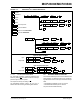
MCP23008/MCP23S08 MCP23008 I2C™ DEVICE PROTOCOL FIGURE 1-1: S - START SR - RESTART S OP DIN W ADDR DIN .... P P - STOP w - Write SR OP R DOUT .... DOUT P OP W DIN DIN P R - Read OP - Device opcode SR ADDR - Device address P DOUT - Data out from MCP23008 DIN .... - Data into MCP23008 OP S DOUT R SR SR OP W OP DOUT .... R ADDR P DOUT .... DOUT P DIN .... DIN P P Byte and Sequential Write Byte S OP W ADDR DIN Sequential S OP W ADDR DIN P DIN .
MCP23008/MCP23S08 1.4.1 ADDRESSING I2C DEVICES (MCP23008) The MCP23008 is a slave I2C device that supports 7-bit slave addressing, with the read/write bit filling out the control byte. The slave address contains four fixed bits and three user-defined hardware address bits (pins A2, A1 and A0). Figure 1-2 shows the control byte format. 1.4.
MCP23008/MCP23S08 1.5 GPIO Port 1.6 The GPIO module contains the data port (GPIO), internal pull up resistors and the Output Latches (OLAT). Configuration and Control Registers The Configuration and Control blocks contain the registers as shown in Table 1-3. Reading the GPIO register reads the value on the port. Reading the OLAT register only reads the OLAT, not the actual value on the port. Writing to the GPIO register actually causes a write to the OLAT.
MCP23008/MCP23S08 1.6.1 I/O DIRECTION (IODIR) REGISTER Controls the direction of the data I/O. When a bit is set, the corresponding pin becomes an input. When a bit is clear, the corresponding pin becomes an output.
MCP23008/MCP23S08 1.6.2 INPUT POLARITY (IPOL) REGISTER The IPOL register allows the user to configure the polarity on the corresponding GPIO port bits. If a bit is set, the corresponding GPIO register bit will reflect the inverted value on the pin.
MCP23008/MCP23S08 1.6.3 INTERRUPT-ON-CHANGE CONTROL (GPINTEN) REGISTER The GPINTEN register controls the interrupt-onchange feature for each pin. If a bit is set, the corresponding pin is enabled for interrupt-on-change. The DEFVAL and INTCON registers must also be configured if any pins are enabled for interrupt-on-change.
MCP23008/MCP23S08 1.6.4 DEFAULT COMPARE (DEFVAL) REGISTER FOR INTERRUPT-ONCHANGE The default comparison value is configured in the DEFVAL register. If enabled (via GPINTEN and INTCON) to compare against the DEFVAL register, an opposite value on the associated pin will cause an interrupt to occur.
MCP23008/MCP23S08 1.6.5 INTERRUPT CONTROL (INTCON) REGISTER The INTCON register controls how the associated pin value is compared for the interrupt-on-change feature. If a bit is set, the corresponding I/O pin is compared against the associated bit in the DEFVAL register. If a bit value is clear, the corresponding I/O pin is compared against the previous value.
MCP23008/MCP23S08 1.6.6 CONFIGURATION (IOCON) REGISTER The IOCON register configuring the device: contains several bits for • The Sequential Operation (SEQOP) controls the incrementing function of the address pointer. If the address pointer is disabled, the address pointer does not automatically increment after each byte is clocked during a serial transfer. This feature is useful when it is desired to continuously poll (read) or modify (write) a register.
MCP23008/MCP23S08 1.6.7 PULL-UP RESISTOR CONFIGURATION (GPPU) REGISTER The GPPU register controls the pull-up resistors for the port pins. If a bit is set and the corresponding pin is configured as an input, the corresponding port pin is internally pulled up with a 100 kΩ resistor.
MCP23008/MCP23S08 1.6.8 INTERRUPT FLAG (INTF) REGISTER Note: The INTF register reflects the interrupt condition on the port pins of any pin that is enabled for interrupts via the GPINTEN register. A ‘set’ bit indicates that the associated pin caused the interrupt. This register is ‘read-only’. Writes to this register will be ignored. REGISTER 1-8: INTF will always reflect the pin(s) that have an interrupt condition. For example, one pin causes an interrupt to occur and is captured in INTCAP and INF.
MCP23008/MCP23S08 1.6.9 INTERRUPT CAPTURE (INTCAP) REGISTER The INTCAP register captures the GPIO port value at the time the interrupt occurred. The register is ‘readonly’ and is updated only when an interrupt occurs. The register will remain unchanged until the interrupt is cleared via a read of INTCAP or GPIO.
MCP23008/MCP23S08 1.6.10 PORT (GPIO) REGISTER The GPIO register reflects the value on the port. Reading from this register reads the port. Writing to this register modifies the Output Latch (OLAT) register.
MCP23008/MCP23S08 1.6.11 OUTPUT LATCH REGISTER (OLAT) The OLAT register provides access to the output latches. A read from this register results in a read of the OLAT and not the port itself. A write to this register modifies the output latches that modify the pins configured as outputs.
MCP23008/MCP23S08 1.7 Interrupt Logic The interrupt output pin will activate if an internal interrupt occurs.
MCP23008/MCP23S08 NOTES: DS21919E-page 22 © 2007 Microchip Technology Inc.
MCP23008/MCP23S08 2.0 ELECTRICAL CHARACTERISTICS Absolute Maximum Ratings † Ambient temperature under bias.............................................................................................................-40°C to +125°C Storage temperature .............................................................................................................................. -65°C to +150°C Voltage on VDD with respect to VSS .................................................................................
MCP23008/MCP23S08 2.1 DC Characteristics DC Characteristics Param No. Operating Conditions (unless otherwise indicated): 1.8V ≤ VDD ≤ 5.5V at -40°C ≤ TA ≤ +85°C (I-Temp) 4.5V ≤ VDD ≤ 5.5V at -40°C ≤ TA ≤ +125°C (E-Temp) (Note 1) Characteristic Sym Min Typ Max Units Conditions D001 Supply Voltage VDD 1.8 — 5.5 V D002 VDD Start Voltage to Ensure Power-on Reset VPOR — VSS — V D003 VDD Rise Rate to Ensure Power-on Reset SVDD 0.
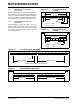
MCP23008/MCP23S08 FIGURE 2-1: LOAD CONDITIONS FOR DEVICE TIMING SPECIFICATIONS VDD Pin 1 kΩ SCL and SDA pin MCP23008 50 pF 135 pF FIGURE 2-2: RESET AND DEVICE RESET TIMER TIMING VDD RESET 30 32 Internal RESET 34 Output pin © 2007 Microchip Technology Inc.
MCP23008/MCP23S08 TABLE 2-1: DEVICE RESET SPECIFICATIONS Operating Conditions (unless otherwise indicated): 1.8V ≤ VDD ≤ 5.5V at -40°C ≤ TA ≤ +85°C (I-Temp) 4.5V ≤ VDD ≤ 5.5V at -40°C ≤ TA ≤ +125°C (E-Temp) (Note 1) AC Characteristics Param No. Characteristic Sym Min Typ(1) Max Units 30 RESET Pulse Width (Low) TRSTL 1 — — µs 32 Device Active After RESET high THLD — 0 — µs 34 Output High-Impedance From RESET Low TIOZ — — 1 µs Note 1: Conditions VDD = 5.
MCP23008/MCP23S08 TABLE 2-2: I2C™ BUS DATA REQUIREMENTS 2 I C™ AC Characteristics Param No. 100 101 Characteristic Operating Conditions (unless otherwise indicated): 1.8V ≤ VDD ≤ 5.5V at -40°C ≤ TA ≤ +85°C (I-Temp) 4.5V ≤ VDD ≤ 5.5V at -40°C ≤ TA ≤ +125°C (E-Temp) (Note 1) RPU (SCL, SDA) = 1 kΩ, CL (SCL, SDA) = 135 pF Min Typ Max 100 kHz mode 4.0 — — µs 1.8V – 5.5V (I-Temp) 400 kHz mode 0.6 — — µs 2.7V – 5.5V (I-Temp) 1.7 MHz mode 0.12 — — µs 4.5V – 5.
MCP23008/MCP23S08 I2C™ BUS DATA REQUIREMENTS (CONTINUED) TABLE 2-2: Operating Conditions (unless otherwise indicated): 1.8V ≤ VDD ≤ 5.5V at -40°C ≤ TA ≤ +85°C (I-Temp) 4.5V ≤ VDD ≤ 5.5V at -40°C ≤ TA ≤ +125°C (E-Temp) (Note 1) RPU (SCL, SDA) = 1 kΩ, CL (SCL, SDA) = 135 pF 2 I C™ AC Characteristics Param No. 109 Characteristic Sym Min Typ Max Output Valid From Clock: TAA 100 kHz mode — — 3.45 µs 1.8V – 5.5V (I-Temp) 400 kHz mode — — 0.9 µs 2.7V – 5.5V (I-Temp) — — 0.18 µs 4.
MCP23008/MCP23S08 FIGURE 2-6: SPI OUTPUT TIMING CS 8 SCK 2 9 Mode 1,1 Mode 0,0 12 SO MSb out LSb out don’t care SI TABLE 2-3: SPI INTERFACE AC CHARACTERISTICS SPI Interface AC Characteristics Param No. 14 13 Characteristic Clock Frequency Operating Conditions (unless otherwise indicated): 1.8V ≤ VDD ≤ 5.5V at -40°C ≤ TA ≤ +85°C (I-Temp) 4.5V ≤ VDD ≤ 5.5V at -40°C ≤ TA ≤ +125°C (E-Temp) (Note 1) Sym Min Typ Max Units Conditions FCLK — — 5 MHz 1.8V – 5.
MCP23008/MCP23S08 TABLE 2-3: SPI INTERFACE AC CHARACTERISTICS (CONTINUED) Operating Conditions (unless otherwise indicated): 1.8V ≤ VDD ≤ 5.5V at -40°C ≤ TA ≤ +85°C (I-Temp) 4.5V ≤ VDD ≤ 5.5V at -40°C ≤ TA ≤ +125°C (E-Temp) (Note 1) SPI Interface AC Characteristics Param No. 9 Characteristic Clock Low Time Sym Min Typ Max Units TLO 90 — — ns Conditions 1.8V – 5.5V (I-Temp) 45 — — ns 2.7V – 5.5V (I-Temp) 45 — — ns 4.5V – 5.
MCP23008/MCP23S08 TABLE 2-4: GP AND INT PINS AC Characteristics Param No. Characteristic Operating Conditions (unless otherwise indicated): 1.8V ≤ VDD ≤ 5.5V at -40°C ≤ TA ≤ +85°C (I-Temp) 4.5V ≤ VDD ≤ 5.
MCP23008/MCP23S08 NOTES: DS21919E-page 32 © 2007 Microchip Technology Inc.
MCP23008/MCP23S08 3.0 PACKAGING INFORMATION 3.1 Package Marking Information 18-Lead PDIP (300 mil) Example: XXXXXXXXXXXXXXXXX XXXXXXXXXXXXXXXXX YYWWNNN 18-Lead SOIC (300 mil) MCP23008-E/P^^ e3 0634256 Example: XXXXXXXXXXXX XXXXXXXXXXXX XXXXXXXXXXXX YYWWNNN 20-Lead QFN 0634256 Example XXXXX XXXXXX XXXXXX YWWNNN 23S08 e3 E/ML^^ 0637 256 20-Lead SSOP Example: XXXXXXXXXXXX XXXXXXXXXXXX YYWWNNN Legend: XX...
MCP23008/MCP23S08 18-Lead Plastic Dual In-Line (P) – 300 mil Body [PDIP] Note: For the most current package drawings, please see the Microchip Packaging Specification located at http://www.microchip.com/packaging N NOTE 1 E1 1 2 3 D E A2 A L c A1 b1 b e eB Units Dimension Limits Number of Pins INCHES MIN N NOM MAX 18 Pitch e Top to Seating Plane A – – .210 Molded Package Thickness A2 .115 .130 .195 Base to Seating Plane A1 .015 – – Shoulder to Shoulder Width E .300 .
MCP23008/MCP23S08 18-Lead Plastic Small Outline (SO) – Wide, 7.50 mm Body [SOIC] Note: For the most current package drawings, please see the Microchip Packaging Specification located at http://www.microchip.com/packaging D N E E1 NOTE 1 1 2 3 b e α h h c φ A2 A A1 β L L1 Units Dimension Limits Number of Pins MILLIMETERS MIN N NOM MAX 18 Pitch e Overall Height A – 1.27 BSC – Molded Package Thickness A2 2.05 – – Standoff § A1 0.10 – 0.
MCP23008/MCP23S08 20-Lead Plastic Quad Flat, No Lead Package (ML) – 4x4x0.9 mm Body [QFN] Note: For the most current package drawings, please see the Microchip Packaging Specification located at http://www.microchip.com/packaging D D2 EXPOSED PAD e E2 2 E b 2 1 1 K N N NOTE 1 TOP VIEW L BOTTOM VIEW A A1 A3 Units Dimension Limits Number of Pins MILLIMETERS MIN N NOM MAX 20 Pitch e Overall Height A 0.80 0.50 BSC 0.90 1.00 Standoff A1 0.00 0.02 0.05 Contact Thickness A3 0.
MCP23008/MCP23S08 20-Lead Plastic Shrink Small Outline (SS) – 5.30 mm Body [SSOP] Note: For the most current package drawings, please see the Microchip Packaging Specification located at http://www.microchip.com/packaging D N E E1 NOTE 1 1 2 b e c A2 A φ A1 L1 Units Dimension Limits Number of Pins L MILLIMETERS MIN N NOM MAX 20 Pitch e Overall Height A – 0.65 BSC – 2.00 Molded Package Thickness A2 1.65 1.75 1.85 Standoff A1 0.05 – – Overall Width E 7.40 7.80 8.
MCP23008/MCP23S08 NOTES: DS21919E-page 38 © 2007 Microchip Technology Inc.
MCP23008/MCP23S08 APPENDIX A: REVISION HISTORY Revision E (August 2007) 1. Section 3.0 “Packaging Information”: Updated package outline drawings. Revision D (February 2007) 1. 2. 3. 4. Changed Byte and Sequential Read in Figure 1-1 from “R” to “W”. Table 2-4, Param No. 51 and 53: Changed from 450 to 600 and 500 to 600, respecively. Added disclaimer to package outline drawings. Updated package outline drawings. Revision C (October 2006) 1. 2. Added 20-pin QFN package information throughout document.
MCP23008/MCP23S08 NOTES: DS21919E-page 40 © 2007 Microchip Technology Inc.
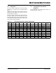
MCP23008/MCP23S08 PRODUCT IDENTIFICATION SYSTEM To order or obtain information, e.g., on pricing or delivery, refer to the factory or the listed sales office. PART NO.
MCP23008/MCP23S08 NOTES: DS21919E-page 42 © 2007 Microchip Technology Inc.
Note the following details of the code protection feature on Microchip devices: • Microchip products meet the specification contained in their particular Microchip Data Sheet. • Microchip believes that its family of products is one of the most secure families of its kind on the market today, when used in the intended manner and under normal conditions. • There are dishonest and possibly illegal methods used to breach the code protection feature.
WORLDWIDE SALES AND SERVICE AMERICAS ASIA/PACIFIC ASIA/PACIFIC EUROPE Corporate Office 2355 West Chandler Blvd. Chandler, AZ 85224-6199 Tel: 480-792-7200 Fax: 480-792-7277 Technical Support: http://support.microchip.com Web Address: www.microchip.