MCP23018/MCP23S18 16-Bit I/O Expander with Open-Drain Outputs Features • Configurable interrupt source: - Interrupt-on-change from configured defaults or pin change • Polarity inversion register to configure the polarity of the input port data • External reset input • Low standby current: - 1 µA (-40°C ≤ TA ≤ +85°C) - 6 µA (+85°C ≤ TA ≤ +125°C) • Operating voltage: - 1.8V to 5.5V • 16-bit remote bidirectional I/O port: - I/O pins default to input • Open-drain outputs: - 5.
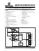
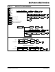
MCP23018/MCP23S18 Package Types: MCP23018 PDIP/SOIC VSS NC GPB0 GPB1 GPB2 GPB3 GPB4 GPB5 GPB6 GPB7 VDD SCL SDA NC 1 2 3 4 5 6 7 8 9 10 11 12 13 14 SSOP 28 27 26 25 24 23 22 21 20 19 18 17 16 15 VSS GPB0 GPB1 GPB2 GPB3 GPB4 GPB5 GPB6 GPB7 VDD SCL SDA NC GPA7 GPA6 GPA5 GPA4 GPA3 GPA2 GPA1 GPA0 INTA INTB NC RESET ADDR 1 2 3 4 5 6 7 8 9 10 11 12 24 23 22 21 20 19 18 17 16 15 14 13 GPA7 GPA6 GPA5 GPA4 GPA3 GPA2 GPA1 GPA0 INTA INTB RESET ADDR QFN 18 GPA3 GPB2 2 17 GPA2 EP 25 GPB3 3 16 GPA1 ADDR 11
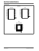
MCP23018/MCP23S18 Package Types: MCP23S18 PDIP/SOIC GPB1 1 GPA4 19 GPA5 20 GPA6 21 18 GPA3 GPB2 2 17 GPA2 EP 25 GPB3 3 16 GPA1 SO 12 13 RESET SI 11 14 INTA * GPB6 6 SCK 10 GPB5 5 CS 9 15 GPA0 VDD 8 GPB4 4 GPB7 7 NC GPA7 GPA6 GPA5 GPA4 GPA3 GPA2 GPA1 GPA0 INTA INTB NC RESET SO GPA7 22 28 27 26 25 24 23 22 21 20 19 18 17 16 15 VSS 23 1 2 3 4 5 6 7 8 9 10 11 12 13 14 GPB0 24 VSS NC GPB0 GPB1 GPB2 GPB3 GPB4 GPB5 GPB6 GPB7 VDD CS SCK SI QFN * * INTB is not bonded out.
MCP23018/MCP23S18 1.0 DEVICE OVERVIEW The MCP23X18 device provides 16-bit, general purpose parallel I/O expansion for I2C bus or SPI applications. The two devices differ only in the serial interface. • MCP23018 - I2C interface • MCP23S18 - SPI interface The MCP23X18 consists of multiple 8-bit configuration registers for input, output and polarity selection. The system master can enable the I/Os as either inputs or outputs by writing the I/O configuration bits.
MCP23018/MCP23S18 1.
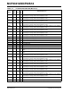
MCP23018/MCP23S18 TABLE 1-2: SPI PINOUT DESCRIPTION (MCP23S18) 28L PDIP/ SOIC 24L QFN Pin Type GPB0 3 24 I/O Bidirectional I/O Pin (5.5 volt tolerant inputs; open-drain outputs). Can be enabled for interrupt on change, and/or internal pull-up resistor.
MCP23018/MCP23S18 1.2 Power-on Reset (POR) The on-chip POR circuit holds the device in reset until VDD has reached a high enough voltage to deactivate the POR circuit (i.e., release the device from reset). The maximum VDD rise time is specified in the electrical specification section. When the device exits the POR condition (releases reset), device operating parameters (i.e., voltage, temperature, serial bus frequency, etc.) must be met to ensure proper operation. 1.
MCP23018/MCP23S18 1.3.2.2 I2C Read Operation 1.3.3 SPI INTERFACE 2 I C read operations include the control byte sequence, as shown in the bottom of Figure 1-1. This sequence is followed by another control byte (including the Start condition and ACK) with the R/W bit equal to a logic one (R/W = 1). The MCP23018 then transmits the data contained in the addressed register. The sequence is ended with the master generating a Stop or Restart condition. 1.3.2.
MCP23018/MCP23S18 MCP23018 I2C™ DEVICE PROTOCOL FIGURE 1-1: S - Start SR - Restart S OP DIN W ADDR DIN .... P P - Stop w - Write DOUT .... SR OP R OP W ADDR .... DOUT P DIN P R - Read OP - Device opcode SR ADDR - Device address P DOUT - Data out from MCP23018 DIN - Data in to MCP23018 OP S DOUT R SR SR OP W OP DOUT .... R ADDR P DOUT .... DOUT P DIN .... DIN P P Byte and Sequential Write Byte S OP W ADDR DIN Sequential S OP W ADDR DIN P ....
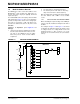
MCP23018/MCP23S18 1.4 Multi-bit Address Decoder The ADDR pin is used to set the slave address of the MCP23018 (I2C only) to allow up to eight devices on the bus using only a single pin. Typically, this would require three pins. The multi-bit Address Decoder employs a basic FLASH ADC architecture (Figure 1-4). The seven comparators generate 8 unique values based on the analog input. This value is converted to a 3-bit code which corresponds to the address bits (A2, A1, A0) in the serial OPCODE.
MCP23018/MCP23S18 FIGURE 1-3: VOLTAGE AND CODE EXAMPLE Assume: n = A2, A1, A0 in opcode ratio = R2/(R1+R2) V2 = voltage on ADDR pin V2(min) = V2 - (VDD/8) x %tolerance V2(max) = V2 + (VDD/8) x %tolerance n R2=2n+1 0 1 2 3 4 5 6 7 n 1 3 5 7 9 11 13 15 R2=2n+1 0 1 2 3 4 5 6 7 n 1 3 5 7 9 11 13 15 R2=2n+1 0 1 2 3 4 5 6 7 n 1 3 5 7 9 11 13 15 R2=2n+1 0 1 2 3 4 5 6 7 © 2008 Microchip Technology Inc. 1 3 5 7 9 11 13 15 10% Tolerance (total) VDD= 1.8 R1=16-R2 R2/(R1+R2) V2 V2(min) V2(max) 0.
MCP23018/MCP23S18 FIGURE 1-4: FLASH ADC BLOCK DIAGRAM VDD analog_in addr_out[6] adc_en addr_out[5] d adc_en adc_en addr_out[4] q addr[6:0] i2c_addr[2:0] en reset '0' set d q adc_en adc_en addr_out[3] i2c_clk adc_en addr_out[2] adc_en addr_out[1] adc_en addr_out[0] adc_en adc_en gnd DS22103A-page 12 © 2008 Microchip Technology Inc.
MCP23018/MCP23S18 FIGURE 1-5: HARDWARE ADDRESS DECODE TIMING tADEN VDD tADDRLAT adc_en i2c_addr[2:0] tADDIS i2c_clk 1.4.2 ADDRESSING I2C DEVICES (MCP23018) The MCP23018 is a slave I2C device that supports 7bit slave addressing, with the read/write bit filling out the control byte. The slave address contains four fixed bits and three user-defined hardware address bits (pins A2, A1, and A0). Figure 1-6 shows the control byte format. 1.4.
MCP23018/MCP23S18 I2C™ ADDRESSING REGISTERS FIGURE 1-8: S 0 1 0 0 A2 A1 A0 0 ACK A7 A6 A5 A4 A3 A2 A1 A0 ACK R/W = 0 Device Opcode Register Address The ACKs are provided by the MCP23X18. FIGURE 1-9: SPI ADDRESSING REGISTERS CS 0 1 0 0 0 Device Opcode DS22103A-page 14 0 0 R/W A7 A6 A5 A4 A3 A2 A1 A0 Register Address © 2008 Microchip Technology Inc.
MCP23018/MCP23S18 1.5 GPIO Port The pull up resistors are individually configured and can be enabled when the pin is cofigured as an input or output. The GPIO module is a general purpose 16-bit wide bidirectional port which is functionally split into two (2) 8-bit wide ports. Reading the GPIOn register reads the value on the port. Reading the OLATn register only reads the latches, not the actual value on the port. The outputs are open-drain.
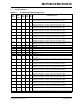
MCP23018/MCP23S18 1.6 Configuration and Control Registers with Port A and ten (10) are associated with Port B. One register (IOCON) is shared between the two ports. The Port A registers are identical to the Port B registers, therefore, they will be referred to without differentiating between the port designation (i.e., they will not have the “A” or “B” designator assigned) in the register tables. There are twenty two (22) registers associated with the MCP23X18 as shown in Table 1-4 and Table 1-5.
MCP23018/MCP23S18 TABLE 1-5: CONTROL REGISTER SUMMARY (IOCON.
MCP23018/MCP23S18 1.6.1 I/O DIRECTION REGISTER Controls the direction of the data I/O. When a bit is set, the corresponding pin becomes an input. When a bit is clear, the corresponding pin becomes an output.
MCP23018/MCP23S18 1.6.2 INPUT POLARITY REGISTER This register allows the user to configure the polarity on the corresponding GPIO port bits. If a bit is set, the corresponding GPIO register bit will reflect the inverted value on the pin.
MCP23018/MCP23S18 1.6.3 INTERRUPT-ON-CHANGE CONTROL REGISTER The GPINTEN register controls the interrupt-onchange feature for each pin. If a bit is set, the corresponding pin is enabled for interrupt-on-change. The DEFVAL and INTCON registers must also be configured if any pins are enabled for interrupt-on-change.
MCP23018/MCP23S18 1.6.4 DEFAULT COMPARE REGISTER FOR INTERRUPT-ON-CHANGE The default comparison value is configured in the DEFVAL register. If enabled (via GPINTEN and INTCON) to compare against the DEFVAL register, an opposite value on the associated pin will cause an interrupt to occur.
MCP23018/MCP23S18 1.6.5 INTERRUPT CONTROL REGISTER The INTCON register controls how the associated pin value is compared for the interrupt-on-change feature. If a bit is set, the corresponding I/O pin is compared against the associated bit in the DEFVAL register. If a bit value is clear, the corresponding I/O pin is compared against the previous value.
MCP23018/MCP23S18 1.6.6 CONFIGURATION REGISTER The IOCON register configuring the device: contains several bits for The BANK bit changes how the registers are mapped (see Table 1-4 and Table 1-5 for more details). • If BANK = 1, the registers associated with each port are segregated. Registers associated with PORTA are are mapped from address 00h - 0Ah and registers associated with PORTB are mapped from Address 10h - 1Ah • If BANK = 0, the A/B registers are paired.
MCP23018/MCP23S18 REGISTER 1-8: IOCON – I/O EXPANDER CONFIGURATION REGISTER R/W-0 BANK R/W-0 R/W-0 U-0 U-0 R/W-0 R/W-0 R/W-0 MIRROR SEQOP - - ODR INTPOL INTCC bit 7 bit 0 Legend: R = Readable bit W = Writable bit U = Unimplemented bit, read as ‘0’ -n = Value at POR ‘1’ = Bit is set ‘0’ = Bit is cleared x = Bit is unknown bit 7 BANK: Controls how the registers are addressed (see Figure 1-4 and Figure 1-5) 1 = The registers associated with each port are separated into different bank
MCP23018/MCP23S18 1.6.7 PULL-UP RESISTOR CONFIGURATION REGISTER The GPPU register controls the pull-up resistors for the port pins. If a bit is set the corresponding port pin is internally pulled up with an internal resistor.
MCP23018/MCP23S18 1.6.8 INTERRUPT FLAG REGISTER The INTF register reflects the interrupt condition on the port pins of any pin that is enabled for interrupts via the GPINTEN register. A ‘set’ bit indicates that the associated pin caused the interrupt. This register is ‘read only’. Writes to this register will be ignored.
MCP23018/MCP23S18 1.6.9 INTERRUPT CAPTURE REGISTER The INTCAP register captures the GPIO port value at the time the interrupt occurred. The register is ‘read only’ and is updated only when an interrupt occurs. The register will remain unchanged until the interrupt is cleared via a read of INTCAP or GPIO.
MCP23018/MCP23S18 1.6.10 PORT REGISTER The GPIO register reflects the value on the port. Reading from this register reads the port. Writing to this register modifies the Output Latch (OLAT) register.
MCP23018/MCP23S18 1.6.11 OUTPUT LATCH REGISTER (OLAT) The OLAT register provides access to the output latches. A read from this register results in a read of the OLAT and not the port itself. A write to this register modifies the output latches that modifies the pins configured as outputs.
MCP23018/MCP23S18 1.7 Interrupt Logic 1.7.2 If enabled, the MCP23X18 activates the INTn interrupt output when one of the port pins changes state or when a pin does not match the pre-configured default. Each pin is individually configurable as follows: • Enable/disable interrupt via GPINTEN • Can interrupt on either pin change or change from default as configured in DEFVAL Both conditions are referred to as Interrupt on Change (IOC).
MCP23018/MCP23S18 1.7.6 INTERRUPT CONDITIONS FIGURE 1-11: INTERRUPT-ON-PINCHANGE There are two possible configurations to cause interrupts (configured via INTCON): 1. 2. Pins configured for interrupt-on-pin-change will cause an interrupt to occur if a pin changes to the opposite state. The default state is reset after an interrupt occurs. For example, an interrupt occurs by an input changing from 1 to 0. The new initial state for the pin is a logic 0.
MCP23018/MCP23S18 NOTES: DS22103A-page 32 © 2008 Microchip Technology Inc.
MCP23018/MCP23S18 2.0 ELECTRICAL CHARACTERISTICS Absolute Maximum Ratings (†) Ambient temperature under bias.............................................................................................................-40°C to +125°C Storage temperature .............................................................................................................................. -65°C to +150°C Voltage on VDD with respect to VSS ...............................................................................
MCP23018/MCP23S18 2.1 DC CHARACTERISTICS DC Characteristics Param No. Characteristic Operating Conditions (unless otherwise indicated): 1.8V ≤ VDD ≤ 5.5V at -40°C ≤ TA ≤ +125°C Sym Min Typ( 2) Max Units D001 Supply Voltage VDD 1.8 — 5.5 V D002 VDD Start Voltage to Ensure Power-on Reset VPOR — VSS — V D003 VDD Rise Rate to Ensure Power-on Reset SVDD 0.05 — — V/ms Conditions Design guidance only. Not tested.
MCP23018/MCP23S18 2.2 AC CHARACTERISTICS FIGURE 2-1: LOAD CONDITIONS FOR DEVICE TIMING SPECIFICATIONS VDD Pin 1 kΩ SCL and SDA pin MCP23018 50 pF 135 pF RESET AND DEVICE RESET TIMER TIMING FIGURE 2-2: VDD RESET 30 32 31 Internal RESET 34 Output pin TABLE 2-1: RESET AND DEVICE RESET TIMER REQUIREMENTS AC Characteristics Standard Operating Conditions (unless otherwise specified) 1.8V ≤ VDD ≤ 5.5V at -40°C ≤ TA ≤ +125°C. Parameter No.
MCP23018/MCP23S18 TABLE 2-2: GP AND INT PINS AC Characteristics Standard Operating Conditions (unless otherwise specified) 1.8V ≤ VDD ≤ 5.5V at -40°C ≤ TA ≤ +125°C. Parameter No.
MCP23018/MCP23S18 TABLE 2-3: HARDWARE ADDRESS LATCH TIMING AC Characteristics Parameter No. Sym 40 tADEN 41 Characteristic Time from VDD stable after POR to ADC enable tADDRLAT Time from ADC enable to address decode and latch 42 Note 1: 2: Standard Operating Conditions (unless otherwise specified) 1.8V ≤ VDD ≤ 5.5V at -40°C ≤ TA ≤ +125°C.
MCP23018/MCP23S18 FIGURE 2-5: I2C BUS START/STOP BITS TIMING SCL 93 91 90 92 SDA STOP Condition START Condition Note 1: Refer to Figure 2-1 for load conditions. FIGURE 2-6: I2C BUS DATA TIMING 103 102 100 101 SCL 90 106 91 107 92 SDA In 109 109 110 SDA Out Note 1: Refer to Figure 2-1 for load conditions. DS22103A-page 38 © 2008 Microchip Technology Inc.
MCP23018/MCP23S18 TABLE 2-4: I2C BUS DATA REQUIREMENTS (SLAVE MODE) I2C™ AC Characteristics Param No. 100 Characteristic Operating Conditions (unless otherwise indicated): 1.8V ≤ VDD ≤ 5.5V at -40°C ≤ TA ≤ +125°C RPU (SCL, SDA) = 1 kΩ, CL (SCL, SDA) = 135 pF. Min Typ Max Units 4.0 — — µs 1.8V – 5.5V 400 kHz mode 0.6 — — µs 1.8V – 5.5V 3.4 MHz mode 0.06 — — µs 2.7V – 5.5V 100 kHz mode 4.7 — — µs 1.8V – 5.5V 400 kHz mode 1.3 — — µs 1.8V – 5.5V 3.4 MHz mode 0.
MCP23018/MCP23S18 I2C BUS DATA REQUIREMENTS (SLAVE MODE) (CONTINUED) TABLE 2-4: Operating Conditions (unless otherwise indicated): 1.8V ≤ VDD ≤ 5.5V at -40°C ≤ TA ≤ +125°C RPU (SCL, SDA) = 1 kΩ, CL (SCL, SDA) = 135 pF. I2C™ AC Characteristics Param No. Characteristic 109 Min Typ Max Units 100 kHz mode — — 3.45 µs 400 kHz mode — — 0.9 µs 1.8V – 5.5V 3.4 MHz mode — — 0.18 µs 2.7V – 5.5V 4.7 — — µs 1.8V – 5.5V 1.3 — — µs 1.8V – 5.5V N/A — N/A µs 2.7V – 5.
MCP23018/MCP23S18 FIGURE 2-8: SPI OUTPUT TIMING CS 8 2 9 SCK Mode 1,1 Mode 0,0 12 13 SO MSB out SI © 2008 Microchip Technology Inc.
MCP23018/MCP23S18 TABLE 2-5: SPI INTERFACE AC CHARACTERISTICS SPI Interface AC Characteristics Param No. Characteristic Operating Conditions (unless otherwise indicated): 1.8V ≤ VDD ≤ 5.5V at -40°C ≤ TA ≤ +125°C. Sym Min Typ Max Units Clock Frequency FCLK — — 10 MHz 1 CS Setup Time TCSS 50 — — ns 2 CS Hold Time TCSH 50 — — ns 1.8V – 5.5V 3 CS Disable Time TCSD 50 — — ns 1.8V – 5.5V 4 Data Setup Time TSU 10 — — ns 1.8V – 5.
MCP23018/MCP23S18 3.0 PACKAGING INFORMATION 3.1 Package Marking Information 24-Lead QFN Example XXXXX XXXXXX XXXXXX YWWNNN 23018 e3 E/MJ^^ 0838 256 24-Lead SSOP (MCP23018 only) XXXXXXXXXXXX XXXXXXXXXXXX YYWWNNN Legend: XX...
MCP23018/MCP23S18 Package Marking Information (Continued) 28-Lead SPDIP (300 mil) Example: XXXXXXXXXXXXXXXXX XXXXXXXXXXXXXXXXX YYWWNNN 28-Lead SOIC (300 mil) XXXXXXXXXXXXXXXXXXXX XXXXXXXXXXXXXXXXXXXX XXXXXXXXXXXXXXXXXXXX YYWWNNN DS22103A-page 44 MCP23018 e3 E/SP^^ 0838256 Example: MCP23018 E/SO^^ e3 YYWW NNN © 2008 Microchip Technology Inc.
MCP23018/MCP23S18 24-Lead Plastic Quad Flat, No Lead Package (MJ) – 4x4x0.9 mm Body [QFN] Note: For the most current package drawings, please see the Microchip Packaging Specification located at http://www.microchip.com/packaging © 2008 Microchip Technology Inc.
MCP23018/MCP23S18 ! " ())$$$ ) DS22103A-page 46 # $ " % & " ' # © 2008 Microchip Technology Inc.
MCP23018/MCP23S18 ! " # $ % ! " ())$$$ ) # $ " % & " ' # D N E E1 1 2 NOTE 1 b e c φ A2 A A1 L L1 5 6 7! / ' & 66 0 0* 7 7 78 9 & :, 3 4 8- ; < < + :, + , + , # '' + , < < 8- = # 0 # # & " # # & " " 0+ ,
MCP23018/MCP23S18 & # ' ( !! " # $ '( % ! " ())$$$ ) # $ " % & " ' # N NOTE 1 E1 1 2 3 D E A2 A L c b1 A1 b e eB 5 6 7! / ' & 74;0 7 7 78 9 & + 3 4 & < < + +1, +, + +, < < ! # ! # = # 0 1+ 11, # # & " # # & " 3
MCP23018/MCP23S18 & ) * + ! " # $ (,% ! " ())$$$ ) # $ " % & " ' # D N E E1 NOTE 1 1 2 3 e b h α A2 A h c φ L A1 β L1 5 6 7! / ' & 66 0 0* 7 7 + 3 4 8- ; " # '' ? 8- = # # # & " 9 & # # & " 78 < < , < < + + < 1 0 = # 8- 6 :,
MCP23018/MCP23S18 NOTES: DS22103A-page 50 © 2008 Microchip Technology Inc.
MCP23018/MCP23S18 APPENDIX A: REVISION HISTORY Revision A (September 2008) • Original Release of this Document. © 2008 Microchip Technology Inc.
MCP23018/MCP23S18 NOTES: DS22103A-page 52 © 2008 Microchip Technology Inc.
MCP23018/MCP23S18 PRODUCT IDENTIFICATION SYSTEM To order or obtain information, e.g., on pricing or delivery, refer to the factory or the listed sales office. PART NO.
MCP23018/MCP23S18 NOTES: DS22103A-page 54 © 2008 Microchip Technology Inc.
Note the following details of the code protection feature on Microchip devices: • Microchip products meet the specification contained in their particular Microchip Data Sheet. • Microchip believes that its family of products is one of the most secure families of its kind on the market today, when used in the intended manner and under normal conditions. • There are dishonest and possibly illegal methods used to breach the code protection feature.
WORLDWIDE SALES AND SERVICE AMERICAS ASIA/PACIFIC ASIA/PACIFIC EUROPE Corporate Office 2355 West Chandler Blvd. Chandler, AZ 85224-6199 Tel: 480-792-7200 Fax: 480-792-7277 Technical Support: http://support.microchip.com Web Address: www.microchip.