
Datasheet
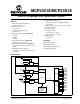

MCP23018/MCP23S18
DS22103A-page 10 © 2008 Microchip Technology Inc.
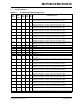
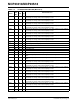
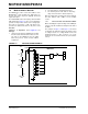
1.4 Multi-bit Address Decoder
The ADDR pin is used to set the slave address of the
MCP23018 (I
2
C only) to allow up to eight devices on
the bus using only a single pin. Typically, this would
require three pins.
The multi-bit Address Decoder employs a basic FLASH
ADC architecture (Figure 1-4). The seven comparators
generate 8 unique values based on the analog input.
This value is converted to a 3-bit code which corre-
sponds to the address bits (A2, A1, A0) in the serial
OPCODE.
Sequence of Operation (see Figure 1-5 for
timings):
1. Upon power up (after V
DD stabilizes) the module
becomes active after time tADEN. Note, the ana-
log value on the ADDR pin must be stable
before this point to ensure accurate address
assignment.
2. The 3-bit address is latched after t
ADDRLAT
.
3. The module powers down after the first rising
edge of the serial clock is detected (t
ADDIS).
Once the address bits are latched, the device will keep
the slave address until a POR or reset condition
occurs.
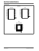
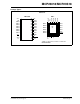
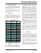
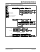
1.4.1 CALCULATING VOLTAGE ON ADDR
When calculating the required voltage on the ADDR pin
(V2), the set point should be the mid-point of the LSb of
the ADC.
The examples in Figure 1-2 and Figure 1-3 show how
to determine the mid point voltage (V2) and the range
of voltages based on a voltage divider circuit. The
maximum tolerance is 20%, however, it is recom-
mended to use 5% tolerance worst case (10% total tol-
erance).
FIGURE 1-2: VOLTAGE DIVIDER EXAMPLE
R2
A0
A1
A2
V2
R1
VDD
MCP23018
VDD
VSS
VSS
ADDR