
Datasheet

© 2008 Microchip Technology Inc. DS22103A-page 7
MCP23018/MCP23S18
1.2 Power-on Reset (POR)
The on-chip POR circuit holds the device in reset until
V
DD has reached a high enough voltage to deactivate
the POR circuit (i.e., release the device from reset).
The maximum VDD rise time is specified in the
electrical specification section.
When the device exits the POR condition (releases
reset), device operating parameters (i.e., voltage,
temperature, serial bus frequency, etc.) must be met to
ensure proper operation.
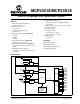
1.3 Serial Interface
This block handles the functionality of the I
2
C
(MCP23018) or SPI (MCP23S18) interface protocol.
The MCP23X18 contains twenty two (22) individual
registers (eleven [11] register pairs) which can be
addressed through the Serial Interface block (Table 1-
1).
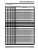
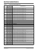
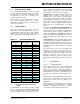
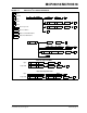
TABLE 1-1: REGISTER ADDRESSES
1.3.1 BYTE MODE AND SEQUENTIAL
MODE
The MCP23X18 has the ability to operate in “Byte
Mode” or “Sequential Mode” (IOCON.SEQOP). Byte
mode and sequential mode are not to be confused with
I
2
C byte operations and sequential operations. The
modes explained here relate to the device’s internal
address pointer and whether or not it is incremented
after each byte is clocked on the serial interface.
Byte Mode disables automatic address pointer incre-
menting. When operating in Byte Mode, the
MCP23X18 does not increment its internal address
counter after each byte during the data transfer. This
gives the ability to continually access the same address
by providing extra clocks (without additional control
bytes). This is useful for polling the GPIO register for
data changes or for continually writing to the output
latches.
A special mode (Byte Mode with IOCON.BANK = 0)
causes the address pointer to toggle between associ-
ated A/B register pairs. For example, if the BANK bit is
cleared and the address pointer is initially set to
address 12h (GPIOA) or 13h (GPIOB), the pointer will
toggle between GPIOA and GPIOB. Note, the address
pointer can initially point to either address in the regis-
ter pair.
Sequential Mode enables automatic address pointer
incrementing. When operating in Sequential Mode, the
MCP23X18 increments its address counter after each
byte during the data transfer. The address pointer auto-
matically rolls over to address 00h after accessing the
last register.
These two modes are not to be confused with single
writes/reads and continuous writes/reads which are
serial protocol sequences. For example, the device
may be configured for Byte Mode and the master may
perform a continuous read. In this case, the
MCP23X18 would not increment the address pointer
and would repeatedly drive data from the same loca-
tion.
1.3.2 I
2
C INTERFACE
1.3.2.1 I
2
C Write Operation
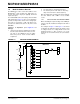
The I
2
C write operation includes the control byte and
register address sequence, as shown in the bottom of
Figure 1-1. This sequence is followed by eight bits of
data from the master and an Acknowledge (ACK) from
the MCP23018. The operation is ended with a stop (P)
or restart (SR) condition being generated by the mas-
ter.
Data is written to the MCP23018 after every byte trans-
fer. If a stop or restart condition is generated during a
data transfer, the data will not be written to the
MCP23018.
Both “byte mode” and “sequential mode” are supported
by the MCP23018. If sequential mode is enabled
(default), the MCP23018 increments its address
counter after each ACK during the data transfer.
Address
IOCON.BANK = 1
Address
IOCON.BANK = 0
Access to:
00h 00h IODIRA
10h 01h IODIRB
01h 02h IPOLA
11h 03h IPOLB
02h 04h GPINTENA
12h 05h GPINTENB
03h 06h DEFVALA
13h 07h DEFVALB
04h 08h INTCONA
14h 09h INTCONB
05h 0Ah IOCON
15h 0Bh IOCON
06h 0Ch GPPUA
16h 0Dh GPPUB
07h 0Eh INTFA
17h 0Fh INTFB
08h 10h INTCAPA
18h 11h INTCAPB
09h 12h GPIOA
19h 13h GPIOB
0Ah 14h OLATA
1Ah 15h OLATB