
Datasheet
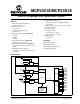

MCP23018/MCP23S18
DS22103A-page 8 © 2008 Microchip Technology Inc.
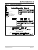
1.3.2.2 I
2
C Read Operation
I
2
C read operations include the control byte sequence,
as shown in the bottom of Figure 1-1. This sequence is
followed by another control byte (including the Start
condition and ACK) with the R/W bit equal to a logic
one (R/W = 1). The MCP23018 then transmits the data
contained in the addressed register. The sequence is
ended with the master generating a Stop or Restart
condition.
1.3.2.3 I
2
C Sequential Write/Read
For sequential operations (Write or Read), instead of
transmitting a Stop or Restart condition after the data
transfer, the master clocks the next byte pointed to by
the address pointer (see Section 1.3.1 “Byte Mode
and Sequential Mode” for details regarding sequential
operation control).
The sequence ends with the master sending a Stop or
Restart condition.
The MCP23018 address pointer will roll over to
address zero after reaching the last register address.
Refer to Figure 1-1.
1.3.3 SPI INTERFACE
1.3.3.1 SPI Write Operation
The SPI write operation is started by lowering CS. The
write command (slave address with R/W bit cleared) is
then clocked into the device. The opcode is followed by
an address and at least one data byte.
1.3.3.2 SPI Read Operation
The SPI read operation is started by lowering CS. The
SPI read command (slave address with R/W bit set) is
then clocked into the device. The opcode is followed by
an address, with at least one data byte being clocked
out of the device.
1.3.3.3 SPI Sequential Write/Read
For sequential operations, instead of deselecting the
device by raising CS, the master clocks the next byte
pointed to by the address pointer. (see Section 1.3.1
“Byte Mode and Sequential Mode” for details regard-
ing sequential operation control).
The sequence ends by the raising of CS
.
The MCP23S18 address pointer will roll over to
address zero after reaching the last register address.