MCP2510 Stand-Alone CAN Controller with SPI™ Interface Features Description • Implements Full CAN V2.0A and V2.
MCP2510 Table of Contents 1.0 Device Functionality . . . . . . . . . . . . . . . . . . . . . . . . . . . . . . . . . . . . . . . . . . . . . . . . . . . . . . . . . . . . . . . . . . . . . . . . . . . . . . . 3 2.0 Can Message Frames. . . . . . . . . . . . . . . . . . . . . . . . . . . . . . . . . . . . . . . . . . . . . . . . . . . . . . . . . . . . . . . . . . . . . . . . . . . . . . 7 3.0 Message Transmission . . . . . . . . . . . . . . . . . . . . . . . . . . . . . . . . . . . . . . . . . . . . . . . .
MCP2510 1.0 DEVICE FUNCTIONALITY 1.1 Overview checked for errors and then matched against the user defined filters to see if it should be moved into one of the two receive buffers. The MCU interfaces to the device via the SPI interface. Writing to and reading from all registers is done using standard SPI read and write commands. The MCP2510 is a stand-alone CAN controller developed to simplify applications that require interfacing with a CAN bus.
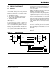
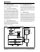
MCP2510 FIGURE 1-2: TYPICAL SYSTEM IMPLEMENTATION Main System Controller MCP2510 CAN Transceiver CAN BUS CAN Transceiver CAN Transceiver CAN Transceiver CAN Transceiver MCP2510 MCP2510 MCP2510 MCP2510 Node Controller Node Controller Node Controller Node Controller SPI INTERFACE TABLE 1-1: PIN DESCRIPTIONS DIP/ SOIC Pin # TSSOP Pin # I/O/P Type TXCAN 1 1 O Transmit output pin to CAN bus RXCAN 2 2 I Receive input pin from CAN bus CLKOUT 3 3 O Clock output pin with programmable
MCP2510 1.2 Transmit/Receive Buffers The MCP2510 has three transmit and two receive buffers, two acceptance masks (one for each receive buffer), and a total of six acceptance filters. Figure 1-3 is a block diagram of these buffers and their connection to the protocol engine.
MCP2510 1.3 CAN Protocol Engine 1.6 The CAN protocol engine combines several functional blocks, shown in Figure 1-4. These blocks and their functions are described below. 1.4 Protocol Finite State Machine The heart of the engine is the Finite State Machine (FSM). This state machine sequences through messages on a bit by bit basis, changing states as the fields of the various frame types are transmitted or received.
MCP2510 2.0 CAN MESSAGE FRAMES The MCP2510 supports Standard Data Frames, Extended Data Frames, and Remote Frames (Standard and Extended) as defined in the CAN 2.0B specification. 2.1 Standard Data Frame The CAN Standard Data Frame is shown in Figure 2-1. In common with all other frames, the frame begins with a Start Of Frame (SOF) bit, which is of the dominant state, which allows hard synchronization of all nodes.
MCP2510 sequence actively violates the bit stuffing rule. All other stations recognize the resulting bit stuffing error and in turn generate error frames themselves, called error echo flags. The error flag field, therefore, consists of between six and twelve consecutive dominant bits (generated by one or more nodes). The error delimiter field completes the error frame. After completion of the error frame, bus activity returns to normal and the interrupted node attempts to resend the aborted message.
© 2007 Microchip Technology Inc.
© 2007 Microchip Technology Inc.
REMOTE DATA FRAME Identifier 11 100 Extended Identifier Message Filtering DLC0 EID0 RTR RB1 RB0 DLC3 4 ID0 SRR IDE EID17 0 15 CRC 7 CRC Del Ack Slot Bit ACK Del 18 ID3 Start of Frame ID10 Arbitration Field 11 16 CRC Field 6 Control Field 32 Reserved bits © 2007 Microchip Technology Inc.
ERROR DATA FRAME Interrupted Data Frame 0 8N (0≤N≤8) Data Field 8 8 DLC0 11 6 Control Field 4 ID0 RTR IDE RB0 DLC3 12 Arbitration Field ID3 Start of Frame ID 10 © 2007 Microchip Technology Inc.
© 2007 Microchip Technology Inc.
MCP2510 NOTES: DS21291F-page 14 © 2007 Microchip Technology Inc.
MCP2510 3.0 MESSAGE TRANSMISSION 3.1 Transmit Buffers The MCP2510 implements three Transmit Buffers. Each of these buffers occupies 14 bytes of SRAM and are mapped into the device memory maps. The first byte, TXBNCTRL, is a control register associated with the message buffer. The information in this register determines the conditions under which the message will be transmitted and indicates the status of the message transmission. (see Register 3-2).
MCP2510 Only messages that have not already begun to be transmitted can be aborted. Once a message has begun transmission, it will not be possible for the user to reset the TXBnCTRL.TXREQ bit. After transmission FIGURE 3-1: of a message has begun, if an error occurs on the bus or if the message loses arbitration, the message will be retransmitted regardless of a request to abort. TRANSMIT MESSAGE FLOWCHART Start No The message transmission sequence begins when the device determines that the TXBnCTRL.
MCP2510 REGISTER 3-1: TXBNCTRL Transmit Buffer N Control Register (ADDRESS: 30h, 40h, 50h) U-0 R-0 R-0 R-0 R/W-0 U-0 R/W-0 R/W-0 — ABTF MLOA TXERR TXREQ — TXP1 TXP0 bit 7 bit 0 bit 7 Unimplemented: Read as '0' bit 6 ABTF: Message Aborted Flag 1 = Message was aborted 0 = Message completed transmission successfully bit 5 MLOA: Message Lost Arbitration 1 = Message lost arbitration while being sent 0 = Message did not lose arbitration while being sent bit 4 TXERR: Transmission Error De
MCP2510 REGISTER 3-2: TXRTSCTRL - TXNRTS PIN CONTROL AND STATUS REGISTER (ADDRESS: 0Dh) U-0 U-0 R-x R-x R-x R/W-0 — — B2RTS B1RTS B0RTS B2RTSM R/W-0 R/W-0 B1RTSM B0RTSM bit 7 bit 0 bit 7 Unimplemented: Read as '0' bit 6 Unimplemented: Read as '0' bit 5 B2RTS: TX2RTS Pin State - Reads state of TX2RTS pin when in digital input mode - Reads as ‘0’ when pin is in ‘request to send’ mode bit 4 B1RTS: TX1RTX Pin State - Reads state of TX1RTS pin when in digital input mode - Reads as ‘0’ wh
MCP2510 REGISTER 3-4: TXBNSIDL - Transmit Buffer N Standard Identifier Low (ADDRESS: 32h, 42h, 52h) R/W-x SID2 R/W-x SID1 R/W-x R/W-x R/W-x R/W-x R/W-x R/W-x SID0 — EXIDE — EID17 EID16 bit 7 bit 0 bit 7-5 SID<2:0>: Standard Identifier Bits <2:0> bit 4 Unimplemented: Reads as '0’ bit 3 EXIDE: Extended Identifier Enable 1 = Message will transmit extended identifier 0 = Message will transmit standard identifier bit 2 Unimplemented: Reads as '0’ bit 1-0 EID<17:16>: Extended Identifier
MCP2510 REGISTER 3-7: TXBNDLC - Transmit Buffer N Data Length Code (ADDRESS: 35h, 45h, 55h) R/W-x R/W-x R/W-x R/W-x R/W-x R/W-x R/W-x R/W-x — RTR — — DLC3 DLC2 DLC1 DLC0 bit 7 bit 0 bit 7 Unimplemented: Reads as '0’ bit 6 RTR: Remote Transmission Request Bit 1 = Transmitted Message will be a Remote Transmit Request 0 = Transmitted Message will be a Data Frame bit 5-4 Unimplemented: Reads as '0’ bit 3-0 DLC<3:0>: Data Length Code Sets the number of data bytes to be transmitted (0 to
MCP2510 4.0 MESSAGE RECEPTION 4.1 Receive Message Buffering The MCP2510 includes two full receive buffers with multiple acceptance filters for each. There is also a separate Message Assembly Buffer (MAB) which acts as a third receive buffer (see Figure 4-1). 4.2 Receive Buffers Of the three Receive Buffers, the MAB is always committed to receiving the next message from the bus. The remaining two receive buffers are called RXB0 and RXB1 and can receive a complete message from the protocol engine.
MCP2510 FIGURE 4-1: RECEIVE BUFFER BLOCK DIAGRAM Acceptance Mask RXM1 Acceptance Filter RXF2 Acceptance Mask RXM0 A c c e p t R X B 0 Acceptance Filter RXF0 Acceptance Filter RXF4 Acceptance Filter RXF1 Acceptance Filter RXF5 Identifier Data Field DS21291F-page 22 Acceptance Filter RXF3 M A B Identifier A c c e p t R X B 1 Data Field © 2007 Microchip Technology Inc.
MCP2510 FIGURE 4-2: MESSAGE RECEPTION FLOWCHART Start Detect Start of Message ? No Yes Begin Loading Message into Message Assembly Buffer (MAB) Generate Error Frame Valid Message Received ? No Yes Yes, meets criteria Yes, meets criteria Message for RXB1 for RXBO Identifier meets a filter criteria ? No Go to Start The CANINTF.RXnIF bit determines if the receive register is empty and able to accept a new message The RXB0CTRL.BUKT bit determines if RXB0 can roll over into RXB1 if it is full Is CANINTF.
MCP2510 REGISTER 4-1: RXB0CTRL - RECEIVE BUFFER 0 CONTROL REGISTER (ADDRESS: 60h) U-0 R/W-0 R/W-0 U-0 R-0 R/W-0 R-0 R-0 — RXM1 RXM0 — RXRTR BUKT BUKT1 FILHIT0 bit 7 bit 0 bit 7 Unimplemented: Read as '0' bit 6-5 RXM<1:0>: Receive Buffer Operating Mode 11 =Turn mask/filters off; receive any message 10 =Receive only valid messages with extended identifiers that meet filter criteria 01 =Receive only valid messages with standard identifiers that meet filter criteria 00 =Receive all valid m
MCP2510 REGISTER 4-2: RXB1CTRL - RECEIVE BUFFER 1 CONTROL REGISTER (ADDRESS: 70h) U-0 R/W-0 R/W-0 U-0 R-0 R-0 R-0 R-0 — RXM1 RXM0 — RXRTR FILHIT2 FILHIT1 FILHIT0 bit 7 bit 0 bit 7 Unimplemented: Read as '0' bit 6-5 RXM<1:0>: Receive Buffer Operating Mode 11 =Turn mask/filters off; receive any message 10 =Receive only valid messages with extended identifiers that meet filter criteria 01 =Receive only valid messages with standard identifiers that meet filter criteria 00 =Receive all vali
MCP2510 REGISTER 4-3: BFPCTRL - RXNBF PIN CONTROL AND STATUS REGISTER (ADDRESS: 0Ch) U-0 U-0 R/W-0 R/W-0 R/W-0 R/W-0 R/W-0 R/W-0 — — B1BFS B0BFS B1BFE B0BFE B1BFM B0BFM bit 7 bit 0 bit 7 Unimplemented: Read as '0' bit 6 Unimplemented: Read as '0' bit 5 B1BFS: RX1BF Pin State (digital output mode only) - Reads as ‘0’ when RX1BF is configured as interrupt pin bit 4 B0BFS: RX0BF Pin State (digital output mode only) - Reads as ‘0’ when RX0BF is configured as interrupt pin bit 3 B1BFE
MCP2510 REGISTER 4-5: RXBNSIDL - RECEIVE BUFFER N STANDARD IDENTIFIER LOW (ADDRESS: 62h, 72h) R-x SID2 R-x SID1 R-x SID0 R-x SRR R-x U-0 R-x R-x IDE — EID17 EID16 bit 7 bit 0 bit 7-5 SID<2:0>: Standard Identifier Bits <2:0> These bits contain the three least significant bits of the Standard Identifier for the received message bit 4 SRR: Standard Frame Remote Transmit Request Bit (valid only if IDE bit = ‘0’) 1 = Standard Frame Remote Transmit Request Received 0 = Standard Data Frame Receiv
MCP2510 REGISTER 4-7: RXBNEID0 - RECEIVE BUFFER N EXTENDED IDENTIFIER LOW (ADDRESS: 64h, 74h) R-x R-x R-x R-x R-x R-x R-x R-x EID7 EID6 EID5 EID4 EID3 EID2 EID1 EID0 bit 7 bit 7-0 bit 0 EID<7:0>: Extended Identifier Bits <7:0> These bits hold the least significant eight bits of the Extended Identifier for the received message Legend: REGISTER 4-8: R = Readable bit W = Writable bit U = Unimplemented bit, read as ‘0’ -n = Value at POR ’1’ = Bit is set ’0’ = Bit is cleared x = Bit is
MCP2510 4.5 Message Acceptance Filters and Masks The Message Acceptance Filters And Masks are used to determine if a message in the message assembly buffer should be loaded into either of the receive buffers (see Figure 4-3). Once a valid message has been received into the MAB, the identifier fields of the message are compared to the filter values. If there is a match, that message will be loaded into the appropriate receive buffer.
MCP2510 FIGURE 4-3: MESSAGE ACCEPTANCE MASK AND FILTER OPERATION Acceptance Filter Register RXFn0 Acceptance Mask Register RXMn0 RXMn1 RXFn1 RXFnn RxRqst RXMnn Message Assembly Buffer Identifier REGISTER 4-10: RXFNSIDH - ACCEPTANCE FILTER N STANDARD IDENTIFIER HIGH (ADDRESS: 00h, 04h, 08h, 10h, 14h, 18h) R/W-x R/W-x R/W-x R/W-x R/W-x R/W-x R/W-x R/W-x SID10 SID9 SID8 SID7 SID6 SID5 SID4 SID3 bit 7 bit 7-0 bit 0 SID<10:3>: Standard Identifier Filter Bits <10:3> These bits hold the
MCP2510 REGISTER 4-11: RXFNSIDL - ACCEPTANCE FILTER N STANDARD IDENTIFIER LOW (ADDRESS: 01h, 05h, 09h, 11h, 15h, 19h) R/W-x SID2 R/W-x SID1 R/W-x U-0 R/W-x U-0 R/W-x R/W-x SID0 — EXIDE — EID17 EID16 bit 7 bit 0 bit 7-5 SID<2:0>: Standard Identifier Filter Bits <2:0> These bits hold the filter bits to be applied to bits <2:0> of the Standard Identifier portion of a received message bit 4 Unimplemented: Reads as '0' bit 3 EXIDE: Extended Identifier Enable 1 = Filter is applied only to Ex
MCP2510 REGISTER 4-13: RXFNEID0 - ACCEPTANCE FILTER N EXTENDED IDENTIFIER LOW (ADDRESS: 03h, 07h, 0Bh, 13h, 17h, 1Bh) R/W-x R/W-x R/W-x R/W-x R/W-x R/W-x R/W-x R/W-x EID7 EID6 EID5 EID4 EID3 EID2 EID1 EID0 bit 7 bit 7-0 bit 0 EID<7:0>: Extended Identifier Bits <7:0> These bits hold the filter bits to be applied to the bits <7:0> of the Extended Identifier portion of a received message Legend: REGISTER 4-14: R = Readable bit W = Writable bit U = Unimplemented bit, read as ‘0’ -n = Val
MCP2510 REGISTER 4-16: RXMNEID8 - ACCEPTANCE FILTER MASK N EXTENDED IDENTIFIER HIGH (ADDRESS: 22h, 26h) R/W-x R/W-x R/W-x R/W-x R/W-x R/W-x R/W-x R/W-x EID15 EID14 EID13 EID12 EID11 EID10 EID9 EID8 bit 7 bit 7-0 bit 0 EID<15:8>: Extended Identifier Bits <15:8> These bits hold the filter bits to be applied to bits <15:8> of the Extended Identifier portion of a received message Legend: REGISTER 4-17: R = Readable bit W = Writable bit U = Unimplemented bit, read as ‘0’ -n = Value at POR
MCP2510 NOTES: DS21291F-page 34 © 2007 Microchip Technology Inc.
MCP2510 5.0 BIT TIMING All nodes on a given CAN bus must have the same nominal bit rate. The CAN protocol uses Non Return to Zero (NRZ) coding which does not encode a clock within the data stream. Therefore, the receive clock must be recovered by the receiving nodes and synchronized to the transmitters clock.
MCP2510 5.1 Time Quanta The Time Quanta (TQ) is a fixed unit of time derived from the oscillator period. There is a programmable baud-rate prescaler, with integral values ranging from 1 to 64, in addition to a fixed divide by two for clock generation. Time quanta is defined as: T Q = 2* ( Baud Rate + 1 )*TOSC where Baud Rate is the binary value represented by CNF1.
MCP2510 5.7 Synchronization To compensate for phase shifts between the oscillator frequencies of each of the nodes on the bus, each CAN controller must be able to synchronize to the relevant signal edge of the incoming signal. Synchronization is the process by which the DPLL function is implemented. When an edge in the transmitted data is detected, the logic will compare the location of the edge to the expected time (Sync Seg).
MCP2510 FIGURE 5-3: SHORTENING A BIT PERIOD Input Signal Sync Prop Segment Phase Segment 1 Phase Segment 2 ≤ SJW Sample Point Actual Bit Length 5.9 Oscillator Tolerance Nominal Bit Length TQ 5.
MCP2510 5.10 Bit Timing Configuration Registers The configuration registers (CNF1, CNF2, CNF3) control the bit timing for the CAN bus interface. These registers can only be modified when the MCP2510 is in configuration mode (see Section 9.0). 5.10.1 CNF1 The BRP<5:0> bits control the baud rate prescaler. These bits set the length of TQ relative to the OSC1 input frequency, with the minimum length of TQ being 2 OSC1 clock cycles in length (when BRP<5:0> are set to 000000).
MCP2510 REGISTER 5-2: CNF2 - CONFIGURATION REGISTER2 (ADDRESS: 29h) R/W-0 R/W-0 BTLMODE SAM R/W-0 R/W-0 R/W-0 PHSEG12 PHSEG11 PHSEG10 R/W-0 R/W-0 R/W-0 PRSEG2 PRSEG1 PRSEG0 bit 7 bit 0 bit 7 BTLMODE: Phase Segment 2 Bit Time Length 1 = Length of Phase Seg 2 determined by PHSEG22:PHSEG20 bits of CNF3 0 = Length of Phase Seg 2 is the greater of Phase Seg 1 and IPT (2TQ) bit 6 SAM: Sample Point Configuration 1 = Bus line is sampled three times at the sample point 0 = Bus line is sampled onc
MCP2510 6.0 ERROR DETECTION The CAN protocol provides sophisticated error detection mechanisms. The following errors can be detected. 6.1 CRC Error With the Cyclic Redundancy Check (CRC), the transmitter calculates special check bits for the bit sequence from the start of a frame until the end of the data field. This CRC sequence is transmitted in the CRC Field. The receiving node also calculates the CRC sequence using the same formula and performs a comparison to the received sequence.
MCP2510 FIGURE 6-1: ERROR MODES STATE DIAGRAM RESET Error-Active REC > 127 or TEC > 127 128 occurrences of 11 consecutive “recessive” bits REC < 127 or TEC < 127 Error-Passive TEC > 255 Bus-Off REGISTER 6-1: TEC - TRANSMITTER ERROR COUNTER (ADDRESS: 1Ch) R-0 R-0 R-0 R-0 R-0 R-0 R-0 R-0 TEC7 TEC6 TEC5 TEC4 TEC3 TEC2 TEC1 TEC0 bit 7 bit 7-0 bit 0 TEC<7:0>: Transmit Error Count Legend: REGISTER 6-2: R = Readable bit W = Writable bit U = Unimplemented bit, read as ‘0’ -n = Value a
MCP2510 REGISTER 6-3: EFLG - ERROR FLAG REGISTER (ADDRESS: 2Dh) R/W-0 R/W-0 R-0 R-0 R-0 R-0 R-0 R-0 RX1OVR RX0OVR TXBO TXEP RXEP TXWAR RXWAR EWARN bit 7 bit 0 bit 7 RX1OVR: Receive Buffer 1 Overflow Flag - Set when a valid message is received for RXB1 and CANINTF.RX1IF = 1 - Must be reset by MCU bit 6 RX0OVR: Receive Buffer 0 Overflow Flag - Set when a valid message is received for RXB0 and CANINTF.
MCP2510 NOTES: DS21291F-page 44 © 2007 Microchip Technology Inc.
MCP2510 7.0 INTERRUPTS The device has eight sources of interrupts. The CANINTE register contains the individual interrupt enable bits for each interrupt source. The CANINTF register contains the corresponding interrupt flag bit for each interrupt source. When an interrupt occurs the INT pin is driven low by the MCP2510 and will remain low until the Interrupt is cleared by the MCU. An Interrupt can not be cleared if the respective condition still prevails.
MCP2510 7.6 Error Interrupt When the error interrupt is enabled (CANINTE.ERRIE = 1) an interrupt is generated on the INT pin if an overflow condition occurs or if the error state of transmitter or receiver has changed. The Error Flag Register (EFLG) will indicate one of the following conditions. 7.6.
MCP2510 REGISTER 7-1: CANINTE - INTERRUPT ENABLE REGISTER (ADDRESS: 2Bh) R/W-0 R/W-0 R/W-0 R/W-0 R/W-0 R/W-0 R/W-0 R/W-0 MERRE WAKIE ERRIE TX2IE TX1IE TX0IE RX1IE RX0IE bit 7 bit 0 bit 7 MERRE: Message Error Interrupt Enable 1 = Interrupt on error during message reception or transmission 0 = Disabled bit 6 WAKIE: Wakeup Interrupt Enable 1 = Interrupt on CAN bus activity 0 = Disabled bit 5 ERRIE: Error Interrupt Enable (multiple sources in EFLG register) 1 = Interrupt on EFLG error co
MCP2510 REGISTER 7-2: CANINTF - INTERRUPT FLAG REGISTER (ADDRESS: 2Ch) R/W-0 R/W-0 R/W-0 R/W-0 R/W-0 R/W-0 R/W-0 R/W-0 MERRF WAKIF ERRIF TX2IF TX1IF TX0IF RX1IF RX0IF bit 7 bit 0 bit 7 MERRF: Message Error Interrupt Flag 1 = Interrupt pending (must be cleared by MCU to reset interrupt condition) 0 = No interrupt pending bit 6 WAKIF: Wakeup Interrupt Flag 1 = Interrupt pending (must be cleared by MCU to reset interrupt condition) 0 = No interrupt pending bit 5 ERRIF: Error Interrupt F
MCP2510 8.0 OSCILLATOR 8.2 The MCP2510 is designed to be operated with a crystal or ceramic resonator connected to the OSC1 and OSC2 pins. The MCP2510 oscillator design requires the use of a parallel cut crystal. Use of a series cut crystal may give a frequency out of the crystal manufacturers specifications. A typical oscillator circuit is shown in Figure 8-1. The MCP2510 may also be driven by an external clock source connected to the OSC1 pin as shown in Figure 8-2 and Figure 8-3. 8.
MCP2510 FIGURE 8-3: EXTERNAL SERIES RESONANT CRYSTAL OSCILLATOR CIRCUIT 330 kΩ 330 kΩ 74AS04 74AS04 To Other Devices 74AS04 MCP2510 OSC1 0.1 mF XTAL Note 1: Duty cycle restrictions must be observed (see Table 12-2). DS21291F-page 50 © 2007 Microchip Technology Inc.
MCP2510 9.0 MODES OF OPERATION The MCP2510 has five modes of operation. These modes are: 1. 2. 3. 4. 5. Configuration Mode. Normal Mode. Sleep Mode. Listen-Only Mode. Loopback Mode. The operational mode is selected via the CANCTRL. REQOP bits (see Register 9-1). When changing modes, the mode will not actually change until all pending message transmissions are complete.
MCP2510 counters are reset and deactivated in this state. The listen-only mode is activated by setting the mode request bits in the CANCTRL register. 9.4 Loopback Mode This mode will allow internal transmission of messages from the transmit buffers to the receive buffers without actually transmitting messages on the CAN bus. This mode can be used in system development and testing.
MCP2510 REGISTER 9-2: CANSTAT - CAN STATUS REGISTER (ADDRESS: XEh) R-1 R-0 R-0 OPMOD2 OPMOD1 OPMOD0 U-0 R-0 R-0 R-0 U-0 — ICOD2 ICOD1 ICOD0 — bit 7 bit 0 bit 7-5 OPMOD<2:0>: Operation Mode 000 = Device is in Normal Operation Mode 001 = Device is in Sleep Mode 010 = Device is in Loopback Mode 011 = Device is in Listen Only Mode 100 = Device is in Configuration Mode bit 4 Unimplemented: Read as '0' bit 3-1 ICOD<2:0>: Interrupt Flag Code 000 = No Interrupt 001 = Error Interrupt 010 = Wake
MCP2510 NOTES: DS21291F-page 54 © 2007 Microchip Technology Inc.
MCP2510 10.0 REGISTER MAP writing of data. Some specific control and status registers allow individual bit modification using the SPI Bit Modify command. The registers that allow this command are shown as shaded locations in Table 10-1. A summary of the MCP2510 control registers is shown in Table 10-2. The register map for the MCP2510 is shown in Table 10-1. Address locations for each register are determined by using the column (higher order 4 bits) and row (lower order 4 bits) values.
MCP2510 NOTES: DS21291F-page 56 © 2007 Microchip Technology Inc.
MCP2510 11.0 SPI INTERFACE 11.5 11.1 Overview The Read Status Instruction allows single instruction access to some of the often used status bits for message reception and transmission. The MCP2510 is designed to interface directly with the Serial Peripheral Interface (SPI) port available on many microcontrollers and supports Mode 0,0 and Mode 1,1. Commands and data are sent to the device via the SI pin, with data being clocked in on the rising edge of SCK.
MCP2510 FIGURE 11-1: BIT MODIFY Mask byte 0 0 1 1 0 1 0 1 Data byte X X 1 0 X 0 X 1 Previous Register Contents 0 1 0 1 0 0 0 1 Resulting Register 0 1 1 0 0 0 0 1 Contents TABLE 11-1: SPI INSTRUCTION SET Instruction Name Instruction Format Description RESET 1100 0000 Resets internal registers to default state, set configuration mode READ 0000 0011 Read data from register beginning at selected address WRITE 0000 0010 Write data to register beginning at selected address RTS (Request To Send
MCP2510 FIGURE 11-4: REQUEST TO SEND INSTRUCTION CS 0 1 2 3 4 5 6 7 SCK instruction 1 SI 0 0 0 T2 T1 T0 high impedance SO FIGURE 11-5: 0 BIT MODIFY INSTRUCTION CS 0 1 2 3 4 5 6 7 8 9 10 11 12 13 14 15 16 17 18 19 20 21 22 23 24 25 26 27 28 29 30 31 SCK SI data byte mask byte address byte instruction 0 0 0 0 0 1 0 1 A7 6 5 4 3 2 1 A0 7 6 5 4 3 2 1 0 7 6 5 4 3 2 1 0 high impedance SO Note: FIGURE 11-6: Not all registers can be accessed with this command.
MCP2510 FIGURE 11-7: RESET INSTRUCTION CS 0 1 2 3 4 5 6 7 0 0 0 SCK instruction SI 1 0 1 0 high impedance SO FIGURE 11-8: 0 SPI INPUT TIMING 3 CS 11 10 6 1 Mode 1,1 7 2 SCK Mode 0,0 4 5 SI MSB in LSB in high impedance SO FIGURE 11-9: SPI OUTPUT TIMING CS 8 2 9 SCK Mode 1,1 Mode 0,0 12 13 SO SI DS21291F-page 60 MSB out 14 LSB out don’t care © 2007 Microchip Technology Inc.
MCP2510 12.0 ELECTRICAL CHARACTERISTICS 12.1 Absolute Maximum Ratings† VDD.............................................................................................................................................................................7.0V All inputs and outputs w.r.t. VSS ..........................................................................................................-0.6V to VDD +1.0V Storage temperature .............................................................................
MCP2510 TABLE 12-1: DC CHARACTERISTICS Industrial (I): Extended (E): DC Characteristics Param. No. Sym Characteristic TAMB = -40°C to +85°C TAMB = -40°C to +125°C Min Max Units VDD Supply Voltage 3.0 5.5 V VRET Register Retention Voltage 2.4 — V High Level Input Voltage VIH RXCAN Conditions Note 2 VDD+1 V SCK, CS, SI, TXnRTS Pins .7 VDD VDD+1 V OSC1 .85 VDD VDD V RESET .85 VDD VDD V Low Level Input Voltage VIL VDD = 3.0V to 5.5V VDD = 4.5V to 5.
MCP2510 TABLE 12-2: OSCILLATOR TIMING CHARACTERISTICS Oscillator Timing Characteristics Param. No. Note: Sym Characteristic Max Units Conditions 1 1 25 16 MHz MHz 4.5V to 5.5V 3.0V to 4.5V TOSC Clock In Period 40 62.5 1000 1000 ns ns 4.5V to 5.5V 3.0V to 4.5V TDUTY Duty Cycle (External Clock Input) 0.45 0.55 — TOSH / (TOSH + TOSL) This parameter is periodically sampled and not 100% tested.
MCP2510 TABLE 12-5: SPI INTERFACE AC CHARACTERISTICS SPI Interface AC Characteristics Param. No. Sym Characteristic Industrial (I): Extended (E): TAMB = -40°C to +85°C TAMB = -40°C to +125°C Min Max Units — — — 5 4 2.5 MHz MHz MHz VDD = 3.0V to 5.5V VDD = 4.5V to 5.5V Conditions FCLK Clock Frequency 1 TCSS CS Setup Time 100 — ns 2 TCSH CS Hold Time 100 115 180 — — — ns ns ns VDD = 4.5V to 5.5V VDD = 4.5V to 5.5V (E temp) VDD = 3.0V to 4.
MCP2510 13.0 PACKAGING INFORMATION 13.1 Package Marking Information 18-Lead PDIP (300 mil) Example: XXXXXXXXXXXXXXXXX XXXXXXXXXXXXXXXXX YYWWNNN 18-Lead SOIC (300 mil) XXXXXXXXXXXX XXXXXXXXXXXX XXXXXXXXXXXX YYWWNNN 20-Lead TSSOP (4.4 mm) MCP2510-I/P e3 XXXXXXXXXXXXXXXXX 0726NNN Example: MCP2510-I/SO e3 XXXXXXXXXXXX XXXXXXXXXXXX 0737NNN Example: XXXXXXXX MCP2510 e3 XXXXXNNN I/STNNN YYWW 0728 Legend: XX...
MCP2510 18-Lead Plastic Dual In-Line (P) – 300 mil Body [PDIP] Note: For the most current package drawings, please see the Microchip Packaging Specification located at http://www.microchip.com/packaging N NOTE 1 E1 1 2 3 D E A2 A L c A1 b1 b e eB Units Dimension Limits Number of Pins INCHES MIN N Pitch e Top to Seating Plane A NOM MAX 18 .100 BSC – – .210 .195 Molded Package Thickness A2 .115 .130 Base to Seating Plane A1 .015 – – Shoulder to Shoulder Width E .300 .
MCP2510 18-Lead Plastic Small Outline (SO) – Wide, 7.50 mm Body [SOIC] Note: For the most current package drawings, please see the Microchip Packaging Specification located at http://www.microchip.com/packaging D N E E1 NOTE 1 1 2 3 b e α h h c φ A2 A A1 β L L1 Units Dimension Limits Number of Pins MILLMETERS MIN N NOM MAX 18 Pitch e Overall Height A – 1.27 BSC – 2.65 Molded Package Thickness A2 2.05 – – Standoff § A1 0.10 – 0.
MCP2510 20-Lead Plastic Thin Shrink Small Outline (ST) – 4.4 mm Body [TSSOP] Note: For the most current package drawings, please see the Microchip Packaging Specification located at http://www.microchip.com/packaging D N E E1 NOTE 1 1 2 b e c φ A2 A A1 L L1 Units Dimension Limits Number of Pins MILLIMETERS MIN N NOM MAX 20 Pitch e Overall Height A – 0.65 BSC – Molded Package Thickness A2 0.80 1.00 1.05 Standoff A1 0.05 – 0.15 1.
MCP2510 APPENDIX A: REVISION HISTORY Revision F (January 2007) This revision includes updates to the packaging diagrams. © 2007 Microchip Technology Inc.
NOTES: DS21291F-page 70 © 2007 Microchip Technology Inc.
MCP2510 INDEX A Acknowledge Error . . . . . . . . . . . . . . . . . . . . . . . . . . . . . . 41 B BFpctrl - RXnBF Pin Control and Status Register . . . . . . . 26 Bit Error . . . . . . . . . . . . . . . . . . . . . . . . . . . . . . . . . . . . . . . 41 BIT Modify instruction . . . . . . . . . . . . . . . . . . . . . . . . . . . . 59 Bit Modify Instruction . . . . . . . . . . . . . . . . . . . . . . . . . . . . . 57 Bit Timing . . . . . . . . . . . . . . . . . . . . . . . . . . . . . . . . . . . . . .
MCP2510 RXMnSIDL - Acceptance Filter Mask n Standard Identifier Low . . . . . . . . . . . . . . . . . . . . . . . . . . . . . . . . . . . . . . 32 S Sample Point . . . . . . . . . . . . . . . . . . . . . . . . . . . . . . . . . . . 36 Shortening a Bit Period . . . . . . . . . . . . . . . . . . . . . . . . . . . 38 Sleep Mode . . . . . . . . . . . . . . . . . . . . . . . . . . . . . . . . . . . . 51 SPI Interface . . . . . . . . . . . . . . . . . . . . . . . . . . . . . . . . . . .
MCP2510 THE MICROCHIP WEB SITE CUSTOMER SUPPORT Microchip provides online support via our WWW site at www.microchip.com. This web site is used as a means to make files and information easily available to customers.
MCP2510 READER RESPONSE It is our intention to provide you with the best documentation possible to ensure successful use of your Microchip product. If you wish to provide your comments on organization, clarity, subject matter, and ways in which our documentation can better serve you, please FAX your comments to the Technical Publications Manager at (480) 792-4150. Please list the following information, and use this outline to provide us with your comments about this document.
MCP2510 PRODUCT IDENTIFICATION SYSTEM To order or obtain information, e.g., on pricing or delivery, refer to the factory or the listed sales office. X PART NO. Device /XX Temperature Range Package Examples: a) MCP2510-E/P: Extended temperature, Industrial temperature, PDIP package. b) MCP2510-I/P: PDIP package. Device: MCP2510: MCP2510T: CAN Controller w/SPI Interface CAN Controller w/SPI Interface (Tape and Reel) c) MCP2510-E/SO: SOIC package.
MCP2510 NOTES: DS21291F-page 76 © 2007 Microchip Technology Inc.
Note the following details of the code protection feature on Microchip devices: • Microchip products meet the specification contained in their particular Microchip Data Sheet. • Microchip believes that its family of products is one of the most secure families of its kind on the market today, when used in the intended manner and under normal conditions. • There are dishonest and possibly illegal methods used to breach the code protection feature.
WORLDWIDE SALES AND SERVICE AMERICAS ASIA/PACIFIC ASIA/PACIFIC EUROPE Corporate Office 2355 West Chandler Blvd. Chandler, AZ 85224-6199 Tel: 480-792-7200 Fax: 480-792-7277 Technical Support: http://support.microchip.com Web Address: www.microchip.
MCP2510 Stand-Alone CAN Controller with SPI™ Interface 1 1.0 Device Functionality . . . . . . . . . . . . . . . . . . . . . . . . . . . . . . . . . . . . . . . . . . . . . . . . . . . . . . . . . . . . . . . . . . . . . . . . . . . . . . . 3 2.0 Can Message Frames . . . . . . . . . . . . . . . . . . . . . . . . . . . . . . . . . . . . . . . . . . . . . . . . . . . . . . . . . . . . . . . . . . . . . . . . . . . . . 7 3.0 Message Transmission . . . . . . . . . . . . . . . . . . . . . . . . . . . . . . . . .
MCP2510 DS21291F-page 80 © 2007 Microchip Technology Inc.