
Datasheet


MCP3004/3008
DS21295D-page 18 © 2008 Microchip Technology Inc.
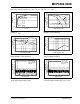
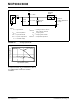
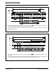
FIGURE 4-1: Analog Input Model.
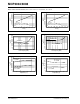
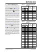
FIGURE 4-2: Maximum Clock Frequency
vs. Input resistance (R
S
) to maintain less than a
0.1 LSB deviation in INL from nominal
conditions.
C
PIN
VA
R
SS
CHx
7pF
V
T
= 0.6V
V
T
= 0.6V
I
LEAKAGE
Sampling
Switch
SS
R
S
= 1 kΩ
C
SAMPLE
= DAC capacitance
V
SS
V
DD
= 20 pF
±1 nA
Legend
VA
=
Signal Source
I
LEAKAGE
=
Leakage Current At The Pin
Due To Various Junctions
R
SS
=
Source Impedance SS
=
sampling switch
CHx
=
Input Channel Pad
R
S
=
sampling switch resistor
C
PIN
=
Input Pin Capacitance
C
SAMPLE
=
sample/hold capacitance
V
T
=
Threshold Voltage
0
1
2
3
4
100 1000 10000
Input Resistance (Ohms)
Clock Frequency (Mhz)
V
DD
= V
REF
= 5 V
f
SAMPLE
= 200 ksps
V
DD
= V
REF
= 2.7 V
f
SAMPLE
= 75 ksps