
Datasheet


MCP3004/3008
DS21295D-page 22 © 2008 Microchip Technology Inc.
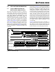
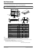
FIGURE 6-2: SPI Communication with the MCP3004/3008 using 8-bit segments (Mode 1,1: SCLK idles high).
6.2 Maintaining Minimum Clock Speed
When the MCP3004/3008 initiates the sample period,
charge is stored on the sample capacitor. When the
sample period is complete, the device converts one bit
for each clock that is received. It is important for the
user to note that a slow clock rate will allow charge to
bleed off the sample capacitor while the conversion is
taking place. At 85°C (worst case condition), the part
will maintain proper charge on the sample capacitor for
at least 1.2 ms after the sample period has ended. This
means that the time between the end of the sample
period and the time that all 10 data bits have been
clocked out must not exceed 1.2 ms (effective clock
frequency of 10 kHz). Failure to meet this criterion may
introduce linearity errors into the conversion outside
the rated specifications. It should be noted that during
the entire conversion cycle, the A/D converter does not
require a constant clock speed or duty cycle, as long as
all timing specifications are met.
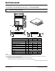
6.3 Buffering/Filtering the Analog
Inputs
If the signal source for the A/D converter is not a low-
impedance source, it will have to be buffered or
inaccurate conversion results may occur (see Figure 4-
2). It is also recommended that a filter be used to
eliminate any signals that may be aliased back in to the
conversion results, as is illustrated in Figure 6-3, where
an op amp is used to drive, filter and gain the analog
input of the MCP3004/3008. This amplifier provides a
low-impedance source for the converter input, plus a
low-pass filter, which eliminates unwanted high-
frequency noise.
Low-pass (anti-aliasing) filters can be designed using
Microchip’s free interactive FilterLab
®
software.
FilterLab will calculate capacitor and resistors values,
as well as determine the number of poles that are
required for the application. For more information on fil-
tering signals, see AN699, “Anti-Aliasing Analog Filters
for Data Acquisition Systems”.
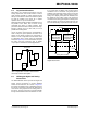
FIGURE 6-3: The MCP601 Operational
Amplifier is used to implement a second order
anti-aliasing filter for the signal being converted
by the MCP3004.
1234567 8 9101112131415 16
CS
SCLK
D
IN
X = “Don’t Care” Bits
17 18 19 20 21 22 23 24
D
OUT
DO
Don’t Care
NULL
BIT
B9
B8
B6 B5 B4 B3 B2 B1 B0
HI-Z
00000
1
XXXXDO
SGL/
DIFF
XXXXX XXX
B7 B6
B5 B4 B3 B2 B1 B0
B9 B8
0
????????
???
MCU latches data from A/D converter
on rising edges of SCLK
Data is clocked out of A/D
converter on falling edges
D1
D2
SGL
/
DIFF
Start
Bit
(Null)
D1
D2
Start
MCU Transmitted Data
(Aligned with falling
edge of clock)
MCU Received Data
(Aligned with rising
edge of clock)
B7
Data stored into MCU receive
register after transmission of first
8 bits
Data stored into MCU receive
register after transmission of
second 8 bits
Data stored into MCU receive
register after transmission of last
8 bits
??
00
MCP3004
V
DD
10 µF
IN-
IN+
-
+
V
IN
C
1
C
2
V
REF
4.096V
Reference
1µF
1µF
0.1 µF
MCP601
R
1
R
2
R
3
R
4
MCP1541