MCP3201 2.7V 12-Bit A/D Converter with SPI Serial Interface Features Description • • • • • • • • • • • • • • The Microchip Technology Inc. MCP3201 device is a successive approximation 12-bit Analog-to-Digital (A/D) Converter with on-board sample and hold circuitry. The device provides a single pseudo-differential input. Differential Nonlinearity (DNL) is specified at ±1 LSB, and Integral Nonlinearity (INL) is offered in ±1 LSB (MCP3201-B) and ±2 LSB (MCP3201-C) versions.
MCP3201 NOTES: DS21290F-page 2 1998-2011 Microchip Technology Inc.
MCP3201 1.0 ELECTRICAL CHARACTERISTICS 1.1 Maximum Ratings† †Notice: Stresses above those listed under “Maximum ratings” may cause permanent damage to the device. This is a stress rating only and functional operation of the device at those or any other conditions above those indicated in the operational listings of this specification is not implied. Exposure to maximum rating conditions for extended periods may affect device reliability. VDD..............................................................
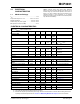
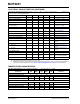
MCP3201 ELECTRICAL CHARACTERISTICS (CONTINUED) Electrical Specifications: All parameters apply at VDD = 5V, VSS = 0V, VREF = 5V, TA = -40°C to +85°C, fSAMPLE = 100 ksps, and fCLK = 16*fSAMPLE, unless otherwise noted. Parameter Sym Min Typ Max Units Conditions High Level Output Voltage VOH 4.1 — — V IOH = -1 mA, VDD = 4.5V Low Level Output Voltage VOL — — 0.4 V IOL = 1 mA, VDD = 4.
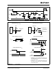
MCP3201 tCSH CS tSUCS tHI tLO CLK tEN HI-Z DOUT FIGURE 1-1: tDO NULL BIT tR tDIS tF MSB OUT HI-Z LSB Serial Timing. Load circuit for tDIS and tEN Load circuit for tR, tF, tDO 1.
MCP3201 NOTES: DS21290F-page 6 1998-2011 Microchip Technology Inc.
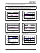
MCP3201 2.0 TYPICAL PERFORMANCE CHARACTERISTICS The graphs provided following this note are a statistical summary based on a limited number of samples and are provided for informational purposes only. The performance characteristics listed herein are not tested or guaranteed. In some graphs, the data presented may be outside the specified operating range (e.g., outside specified power supply range) and therefore outside the warranted range. Note: 1.0 0.8 0.6 0.4 0.2 0.0 -0.2 -0.4 -0.6 -0.8 -1.0 2.
MCP3201 Note: Unless otherwise indicated, VDD = VREF = 5V, VSS = 0V, fSAMPLE = 100 ksps, fCLK = 16*fSAMPLE, TA = +25°C. 1.0 1.0 0.6 0.6 0.4 0.4 0.2 0.0 Negative INL -0.2 VDD = VREF = 2.7V FSAMPLE = 50 ksps 0.8 Positive INL INL (LSB) INL (LSB) 0.8 -0.4 0.2 0.0 -0.2 -0.4 -0.6 -0.6 -0.8 -0.8 Negative INL -1.0 -1.0 -50 -25 0 25 50 75 -50 100 -25 Integral Nonlinearity (INL) 25 50 75 100 FIGURE 2-10: Integral Nonlinearity (INL) vs. Temperature (VDD = 2.7V). 2.0 VDD = VREF = 2.
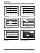
MCP3201 1.0 0.8 0.6 0.4 0.2 0.0 -0.2 -0.4 -0.6 -0.8 -1.0 DNL (LSB) DNL (LSB) Note: Unless otherwise indicated, VDD = VREF = 5V, VSS = 0V, fSAMPLE = 100 ksps, fCLK = 16*fSAMPLE, TA = +25°C. 0 512 1024 1536 2048 2560 3072 3584 4096 Digital Code 1.0 0.8 0.6 0.4 0.2 0.0 -0.2 -0.4 -0.6 -0.8 -1.0 FIGURE 2-16: Differential Nonlinearity (DNL) vs. Code (Representative Part, VDD = 2.7V). Positive DNL DNL (LSB) DNL (LSB) FIGURE 2-13: Differential Nonlinearity (DNL) vs. Code (Representative Part).
MCP3201 Offset Error (LSB) 1.0 0.8 0.6 0.4 0.2 0.0 -0.2 -0.4 -0.6 -0.8 -1.0 VDD = VREF = 2.7V FSAMPLE = 50 ksps VDD = VREF = 5V FSAMPLE = 100 ksps -50 -25 FIGURE 2-19: 0 25 50 Temperature (°C) 75 Gain Error vs. Temperature. 100 90 80 70 60 50 40 30 20 10 0 SNR (dB) VDD = VREF = 2.7V FSAMPLE = 50 ksps 10 Input Frequency (kHz) -25 100 90 80 70 60 50 40 30 20 10 0 0 25 50 Temperature (°C) 75 100 Offset Error vs. VDD = VREF = 5V FSAMPLE = 100 ksps VDD = VREF = 2.
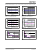
MCP3201 12.0 12.00 11.75 11.50 11.25 11.00 10.75 10.50 10.25 10.00 9.75 9.50 9.25 9.00 VDD = 5V 11.5 FSAMPLE = 100 ksps 11.0 VDD = VREF = 5V FSAMPLE =100 ksps VDD = VREF = 2.7V FSAMPLE = 50 ksps ENOB (rms) ENOB (rms) Note: Unless otherwise indicated, VDD = VREF = 5V, VSS = 0V, fSAMPLE = 100 ksps, fCLK = 16*fSAMPLE, TA = +25°C. 10.5 10.0 9.5 9.0 VDD = 2.7V 8.5 FSAMPLE = 50 ksps 8.0 0.0 0.5 1.0 1.5 2.0 2.5 3.0 3.5 4.0 4.5 5.0 1 10 VREF (V) FIGURE 2-25: (ENOB) vs. VREF.
MCP3201 500 450 400 350 300 250 200 150 100 50 0 100 90 80 70 60 50 40 30 20 10 0 VREF = VDD All points at FCLK = 1.6 MHz, except at VREF = VDD = 2.5V, FCLK = 800 kHz VREF = VDD All points at FCLK = 1.6 MHz, except at VREF = VDD = 2.5V, FCLK = 800 kHz IREF (µA) IDD (µA) Note: Unless otherwise indicated, VDD = VREF = 5V, VSS = 0V, fSAMPLE = 100 ksps, fCLK = 16*fSAMPLE, TA = +25°C. 2.0 2.5 3.0 3.5 4.0 4.5 5.0 5.5 6.0 2.0 2.5 3.0 3.5 V DD (V) FIGURE 2-31: IDD vs. VDD. FIGURE 2-34: 5.
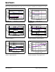
MCP3201 Note: Unless otherwise indicated, VDD = VREF = 5V, VSS = 0V, fSAMPLE = 100 ksps, fCLK = 16*fSAMPLE, TA = +25°C. 70 Analog Input Leakage (nA) 80 VREF = CS = VDD IDDS (pA) 60 50 40 30 20 10 0 2.0 2.5 3.0 FIGURE 2-37: 3.5 4.0 4.5 VDD (V) 5.0 5.5 6.0 IDDS vs. VDD. 2.0 1.8 1.6 1.4 1.2 1.0 0.8 0.6 0.4 0.2 0.0 VDD = VREF = 5V FCLK = 1.6 MHz -50 -25 0 25 50 Temperature (°C) 75 100 FIGURE 2-39: Analog Input Leakage Current vs. Temperature. 100.00 VDD = VREF = CS = 5V I DDS (nA) 10.
MCP3201 NOTES: DS21290F-page 14 1998-2011 Microchip Technology Inc.
MCP3201 3.0 PIN DESCRIPTIONS The descriptions of the pins are listed in Table 3-1. Additional descriptions of the device pins follows. TABLE 3-1: PIN FUNCTION TABLE MCP3201 MSOP, PDIP, SOIC, TSSOP Symbol 1 VREF 2 IN+ Positive Analog Input 3 IN- Negative Analog Input 4 VSS Ground 5 CS/SHDN 3.1 Chip Select/Shutdown Input 6 DOUT Serial Data Out CLK Serial Clock 8 VDD +2.7V to 5.5V Power Supply Positive Analog Input (IN+) Negative Analog Input (IN-) Negative analog input.
MCP3201 NOTES: DS21290F-page 16 1998-2011 Microchip Technology Inc.
MCP3201 4.0 DEVICE OPERATION 4.2 Reference Input The MCP3201 A/D Converter employs a conventional SAR architecture. With this architecture, a sample is acquired on an internal sample/hold capacitor for 1.5 clock cycles starting on the first rising edge of the serial clock after CS has been pulled low. Following this sample time, the input switch of the converter opens and the device uses the collected charge on the internal sample and hold capacitor to produce a serial 12-bit digital output code.
MCP3201 VDD RSS VT = 0.6V CHx CPIN 7 pF VA Sampling Switch VT = 0.6V SS ILEAKAGE ±1 nA RS = 1 k CSAMPLE = DAC capacitance = 20 pF VSS Legend: VA RSS CHx CPIN VT ILEAKAGE SS RS CSAMPLE = = = = = = = = = FIGURE 4-1: Signal Source Source Impedance Input Channel Pad Input Pin Capacitance Threshold Voltage Leakage Current At The Pin Due To Various Junctions Sampling Switch Sampling Switch Resistor Sample/hold Capacitance Analog Input Model. Clock Frequency (MHz) 1.8 1.6 VDD = VREF = 5V 1.4 1.
MCP3201 5.0 SERIAL COMMUNICATIONS Communication with the device is done using a standard SPI-compatible serial interface. Initiating communication with the MCP3201 device begins with the CS going low. If the device was powered up with the CS pin low, it must be brought high and back low to initiate communication. The device will begin to sample the analog input on the first rising edge after CS goes low.
MCP3201 NOTES: DS21290F-page 20 1998-2011 Microchip Technology Inc.
MCP3201 6.0 APPLICATIONS INFORMATION 6.1 Using the MCP3201 Device with Microcontroller SPI Ports device, the microcontroller’s receive buffer will contain two unknown bits (the output is at high-impedance for the first two clocks), the null bit and the highest order five bits of the conversion.
MCP3201 6.2 Maintaining Minimum Clock Speed When the MCP3201 initiates the sample period, charge is stored on the sample capacitor. When the sample period is complete, the device converts one bit for each clock that is received. It is important for the user to note that a slow clock rate will allow charge to bleed off the sample cap while the conversion is taking place. At 85°C (worst-case condition), the part will maintain proper charge on the sample capacitor for at least 1.
MCP3201 6.4 Layout Considerations When laying out a printed circuit board for use with analog components, care should be taken to reduce noise wherever possible. A bypass capacitor should always be used with this device and should be placed as close as possible to the device pin. A bypass capacitor value of 1 µF is recommended. Digital and analog traces should be separated as much as possible on the board and no traces should run underneath the device or the bypass capacitor.
MCP3201 NOTES: DS21290F-page 24 1998-2011 Microchip Technology Inc.
MCP3201 7.0 PACKAGING INFORMATION 7.1 Package Marking Information 8-Lead MSOP (3x3 mm) Example 3201CI 130256 8-Lead PDIP (300 mil) XXXXXXXX XXXXXNNN YYWW 8-Lead SOIC (3.90 mm) NNN 8-Lead TSSOP (4.4 mm) Example 3201-B e3 256 I/P ^^ 1130 Example 3201-BI e3 SN ^^1130 256 Example 201C I130 256 Legend: XX...
MCP3201 1 % & % ! % 2 " ) ' % 2 $ % % " % %% 033))) & &3 2 D N E E1 NOTE 1 1 2 e b A2 A c φ L L1 A1 4 % & 5 & % 6!&( $ 55 * * 6 6 67 8 9 % 7 ; % < < + 9+ + < + " " 2 2 % " $$ :+ . / 7 = "% * " " 2 = "% * , .
MCP3201 Note: For the most current package drawings, please see the Microchip Packaging Specification located at http://www.microchip.com/packaging 1998-2011 Microchip Technology Inc.
MCP3201 ! "## $ % 1 % & % ! % 2 " ) ' % 2 $ % % " % %% 033))) & &3 2 N NOTE 1 E1 1 3 2 D E A2 A L A1 c e eB b1 b 4 % & 5 & % 6!&( $ 6/;* 6 6 % 8 9 % % 67 . / < < + , + .
MCP3201 Note: For the most current package drawings, please see the Microchip Packaging Specification located at http://www.microchip.com/packaging 1998-2011 Microchip Technology Inc.
MCP3201 Note: For the most current package drawings, please see the Microchip Packaging Specification located at http://www.microchip.com/packaging DS21290F-page 30 1998-2011 Microchip Technology Inc.
MCP3201 ! &' "()# $ % * 1 % & % ! % 2 " ) ' % 2 $ % % " % %% 033))) & &3 2 1998-2011 Microchip Technology Inc.
MCP3201 +, , + ! -(- $ % + 1 % & % ! % 2 " ) ' % 2 $ % % " % %% 033))) & &3 2 D N E E1 NOTE 1 1 2 b e c A φ A2 A1 L L1 4 % & 5 & % 6!&( $ 55 * * 6 6 67 8 9 % 7 ; % < < 9 + + < + " " 2 2 % " $$ :+ .
MCP3201 Note: For the most current package drawings, please see the Microchip Packaging Specification located at http://www.microchip.com/packaging 1998-2011 Microchip Technology Inc.
MCP3201 NOTES: DS21290F-page 34 1998-2011 Microchip Technology Inc.
MCP3201 APPENDIX A: REVISION HISTORY Revision F (August 2011) • Updated Product Identification System section. - Corrected marking drawings for MSOP packages. - Updated PDIP, SOIC, and TSSOP package specification drawings. Revision E (November 2008) The following is the list of modifications: 1. 2. Updated Section 7.0 “Packaging Information”. Updated Product Identification System section. Revision D (January 2007) The following is the list of modifications: 1.
MCP3201 NOTES: DS21290F-page 36 1998-2011 Microchip Technology Inc.
MCP3201 PRODUCT IDENTIFICATION SYSTEM To order or obtain information, e.g., on pricing or delivery, refer to the factory or the listed sales office. PART NO.
MCP3201 NOTES: DS21290F-page 38 1998-2011 Microchip Technology Inc.
Note the following details of the code protection feature on Microchip devices: • Microchip products meet the specification contained in their particular Microchip Data Sheet. • Microchip believes that its family of products is one of the most secure families of its kind on the market today, when used in the intended manner and under normal conditions. • There are dishonest and possibly illegal methods used to breach the code protection feature.
Worldwide Sales and Service AMERICAS ASIA/PACIFIC ASIA/PACIFIC EUROPE Corporate Office 2355 West Chandler Blvd. Chandler, AZ 85224-6199 Tel: 480-792-7200 Fax: 480-792-7277 Technical Support: http://www.microchip.com/ support Web Address: www.microchip.