
Datasheet


1998-2011 Microchip Technology Inc. DS21290F-page 23
MCP3201
6.4 Layout Considerations
When laying out a printed circuit board for use with
analog components, care should be taken to reduce
noise wherever possible. A bypass capacitor should
always be used with this device and should be placed
as close as possible to the device pin. A bypass
capacitor value of 1 µF is recommended.
Digital and analog traces should be separated as much
as possible on the board and no traces should run
underneath the device or the bypass capacitor. Extra
precautions should be taken to keep traces with high-
frequency signals (such as clock lines) as far as
possible from analog traces.
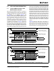
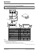
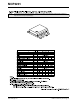
Use of an analog ground plane is recommended in
order to keep the ground potential the same for all
devices on the board. Providing V
DD
connections to
devices in a “star” configuration can also reduce noise
by eliminating current return paths and associated
errors. See Figure 6-4. For more information on layout
tips when using A/D Converter, refer to AN688 “Layout
Tips for 12-Bit A/D Converter Applications”.
FIGURE 6-4: V
DD
traces arranged in a
‘Star’ configuration in order to reduce errors
caused by current return paths.
V
DD
Connection
Device 1
Device 2
Device 3
Device 4