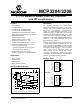
MCP3204/3208 2.7V 4-Channel/8-Channel 12-Bit A/D Converters with SPI Serial Interface Features Description • • • • • • The Microchip Technology Inc. MCP3204/3208 devices are successive approximation 12-bit Analogto-Digital (A/D) Converters with on-board sample and hold circuitry. The MCP3204 is programmable to provide two pseudo-differential input pairs or four single-ended inputs. The MCP3208 is programmable to provide four pseudo-differential input pairs or eight single-ended inputs.
MCP3204/3208 1.0 †Notice: Stresses above those listed under "Maximum Ratings" may cause permanent damage to the device. This is a stress rating only and functional operation of the device at those or any other conditions above those indicated in the operation listings of this specification is not implied. Exposure to maximum rating conditions for extended periods may affect device reliability. ELECTRICAL CHARACTERISTICS Absolute Maximum Ratings† VDD........................................................
MCP3204/3208 ELECTRICAL SPECIFICATIONS (CONTINUED) Electrical Characteristics: Unless otherwise noted, all parameters apply at VDD = 5V, VSS = 0V, VREF = 5V, TA = -40°C to +85°C,fSAMPLE = 100 ksps and fCLK = 20*fSAMPLE Parameters Sym Min Typ Max Units VSS-100 — VSS+100 mV Leakage Current — 0.
MCP3204/3208 TEMPERATURE CHARACTERISTICS Electrical Specifications: Unless otherwise indicated, VDD = 5V, VSS = 0V, VREF = 5V Parameters Sym Min Typ Max Units Specified Temperature Range TA -40 — +125 °C Operating Temperature Range TA -40 — +125 °C Storage Temperature Range TA -65 — +150 °C Thermal Resistance, 14L-PDIP θJA — 70 — °C/W Thermal Resistance, 14L-SOIC θJA — 95.
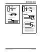
MCP3204/3208 Test Point 1.4V VDD 3 kΩ Test Point 3 kΩ tDIS Waveform 2 VDD/2 tEN Waveform DOUT DOUT 100 pF CL = 100 pF tDIS Waveform 1 VSS Voltage Waveforms for tR, tF Voltage Waveforms for tEN VOH VOL DOUT CS tF tR 1 CLK 2 3 4 Voltage Waveforms for tDO B11 DOUT CLK tEN tDO DOUT Voltage Waveforms for tDIS CS FIGURE 1-2: Load Circuit for tR, tF, tDO.
MCP3204/3208 NOTES: DS21298E-page 6 © 2008 Microchip Technology Inc.
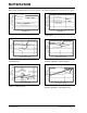
MCP3204/3208 2.0 TYPICAL PERFORMANCE CHARACTERISTICS The graphs and tables provided following this note are a statistical summary based on a limited number of samples and are provided for informational purposes only. The performance characteristics listed herein are not tested or guaranteed. In some graphs or tables, the data presented may be outside the specified operating range (e.g., outside specified power supply range) and therefore outside the warranted range.
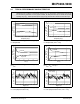
MCP3204/3208 Note: Unless otherwise indicated, VDD = VREF = 5 V, VSS = 0 V, fSAMPLE = 100 ksps, fCLK = 20* fSAMPLE, TA = +25°C. 1.0 1.0 0.6 0.6 0.4 0.4 0.2 0.0 Negative INL -0.2 VDD = VREF = 2.7 V FSAMPLE = 50 ksps 0.8 Positive INL INL (LSB) INL (LSB) 0.8 Positive INL 0.2 0.0 -0.2 -0.4 -0.4 -0.6 -0.6 -0.8 -0.8 Negative INL -1.0 -1.0 -50 -25 0 25 50 75 -50 100 -25 0 Temperature (°C) FIGURE 2-7: vs. Temperature. Integral Nonlinearity (INL) 1.0 2.0 0.8 1.
MCP3204/3208 1.0 1.0 0.8 0.8 0.6 0.6 0.4 0.4 DNL (LSB) DNL (LSB) Note: Unless otherwise indicated, VDD = VREF = 5V, VSS = 0V, fSAMPLE = 100 ksps, fCLK = 20* fSAMPLE, TA = +25°C. 0.2 0.0 -0.2 0.2 0.0 -0.2 -0.4 -0.4 -0.6 -0.6 -0.8 -0.8 -1.0 VDD = VREF = 2.7 V FSAMPLE = 50 ksps -1.0 0 512 1024 1536 2048 2560 3072 3584 4096 0 512 1024 1536 Digital Code 1.0 1.0 0.8 0.8 0.6 DNL (LSB) DNL (LSB) 0.4 0.2 0.0 -0.2 Negative DNL -0.6 3584 4096 Positive DNL 0.2 0.0 -0.
MCP3204/3208 Note: Unless otherwise indicated, VDD = VREF = 5V, VSS = 0V, fSAMPLE = 100 ksps, fCLK = 20* fSAMPLE, TA = +25°C. 2.0 0.2 VDD = VREF = 2.7 V FSAMPLE = 50 ksps -0.2 1.8 Offset Error (LSB) Gain Error (LSB) 0.0 -0.4 -0.6 -0.8 -1.0 VDD = VREF = 5 V FSAMPLE = 100 ksps -1.2 -1.4 VDD = VREF = 5 V FSAMPLE = 100 ksps 1.6 1.4 1.2 1.0 VDD = VREF = 2.7 V FSAMPLE = 50 ksps 0.8 0.6 0.4 0.2 -1.6 0.0 -1.8 -50 -25 0 25 50 75 -50 100 -25 0 Temperature (°C) FIGURE 2-19: Gain Error vs.
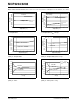
MCP3204/3208 12.0 12.00 11.75 11.50 11.25 11.00 10.75 10.50 10.25 10.00 9.75 9.50 9.25 9.00 11.5 11.0 ENOB (rms) ENOB (rms) Note: Unless otherwise indicated, VDD = VREF = 5V, VSS = 0V, fSAMPLE = 100 ksps, fCLK = 20* fSAMPLE, TA = +25°C. VDD = VREF = 5 V FSAMPLE =100 ksps VDD = VREF = 2.7 V FSAMPLE = 50 ksps 10.5 VDD = VREF = 5 V FSAMPLE = 100 ksps 10.0 9.5 VDD = VREF = 2.7 V FSAMPLE = 50 ksps 9.0 8.5 8.0 0.0 0.5 1.0 1.5 2.0 2.5 3.0 3.5 4.0 4.5 5.0 1 VREF (V) FIGURE 2-25: (ENOB) vs.
MCP3204/3208 Note: Unless otherwise indicated, VDD = VREF = 5V, VSS = 0V, fSAMPLE = 100 ksps, fCLK = 20* fSAMPLE, TA = +25°C. 500 100 VREF = VDD All points at FCLK = 2 MHz, except at VREF = VDD = 2.5 V, FCLK = 1 MHz 450 400 80 70 300 IREF (µA) IDD (µA) 350 VREF = VDD All points at FCLK = 2 MHz except at VREF = VDD = 2.5 V, FCLK = 1 MHz 90 250 200 60 50 40 150 30 100 20 50 10 0 0 2.0 2.5 3.0 3.5 4.0 4.5 5.0 5.5 6.0 2.0 2.5 3.0 3.5 FIGURE 2-31: 4.0 4.5 5.0 5.5 6.
MCP3204/3208 Note: Unless otherwise indicated, VDD = VREF = 5V, VSS = 0V, fSAMPLE = 100 ksps, fCLK = 20* fSAMPLE, TA = +25°C. 2.0 70 Analog Input Leakage (nA) 80 VREF = CS = VDD IDDS (pA) 60 50 40 30 20 10 0 1.8 1.6 1.4 1.2 VDD = VREF = 5 V FCLK = 2 MHz 1.0 0.8 0.6 0.4 0.2 0.0 2.0 2.5 3.0 3.5 4.0 4.5 5.0 5.5 6.0 VDD (V) FIGURE 2-37: -50 -25 0 25 50 75 100 Temperature (°C) FIGURE 2-39: Analog Input Leakage Current vs. Temperature. IDDS vs. VDD. 100.
MCP3204/3208 NOTES: DS21298E-page 14 © 2008 Microchip Technology Inc.
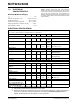
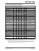
MCP3204/3208 3.0 PIN DESCRIPTIONS The descriptions of the pins are listed in Table 3-1. TABLE 3-1: PIN FUNCTION TABLE MCP3204 MCP3208 PDIP, SOIC, TSSOP PDIP, SOIC 1 1 CH0 Analog Input 2 2 CH1 Analog Input 3 3 CH2 Analog Input 3.
MCP3204/3208 NOTES: DS21298E-page 16 © 2008 Microchip Technology Inc.
MCP3204/3208 4.0 DEVICE OPERATION The MCP3204/3208 A/D converters employ a conventional SAR architecture. With this architecture, a sample is acquired on an internal sample/hold capacitor for 1.5 clock cycles starting on the fourth rising edge of the serial clock after the start bit has been received. Following this sample time, the device uses the collected charge on the internal sample/hold capacitor to produce a serial 12-bit digital output code.
MCP3204/3208 VDD RSS VT = 0.6V CHx CPIN 7 pF VA Sampling Switch SS RS = 1 kΩ ILEAKEAGE ±1 nA VT = 0.6V CSAMPLE = DAC capacitance = 20 pF VSS Legend VA = Signal Source Ileakage = Leakage Current At The Pin Due To Various Junctions Rss = Source Impedance SS = Sampling switch CHx = Input Channel Pad Rs = Sampling switch resistor Cpin = Input Pin Capacitance Csample = Sample/hold capacitance Vt = Threshold Voltage FIGURE 4-1: Analog Input Model. Clock Frequency (MHz) 2.
MCP3204/3208 5.0 SERIAL COMMUNICATIONS Communication with the MCP3204/3208 devices is accomplished using a standard SPI-compatible serial interface. Initiating communication with either device is done by bringing the CS line low (see Figure 5-1). If the device was powered up with the CS pin low, it must be brought high and back low to initiate communication. The first clock received with CS low and DIN high will constitute a start bit.
MCP3204/3208 tCYC tCYC tCSH CS tSUCS CLK SGL/ DIN Start DIFF D2 D1 D0 HI-Z DOUT Start SGL/ DIFF D2 Don’t Care Null Bit B11 B10 B9 B8 B7 B6 B5 B4 B3 B2 B1 B0* HI-Z tCONV tSAMPLE tDATA ** * After completing the data transfer, if further clocks are applied with CS low, the A/D converter will output LSB first data, followed by zeros indefinitely (see Figure 5-2 below).
MCP3204/3208 6.0 APPLICATIONS INFORMATION 6.1 Using the MCP3204/3208 with Microcontroller (MCU) SPI Ports As is shown in Figure 6-1, the first byte transmitted to the A/D converter contains five leading zeros before the start bit. Arranging the leading zeros this way allows the output 12 bits to fall in positions easily manipulated by the MCU. The MSB is clocked out of the A/D converter on the falling edge of clock number 12.
MCP3204/3208 CS MCU latches data from A/D converter on rising edges of SCLK SCLK 1 2 3 4 5 6 7 8 9 10 11 12 13 14 15 16 17 18 19 20 21 22 23 24 Data is clocked out of A/D converter on falling edges SGL/ DIN Start DIFF FIGURE 6-2: 6.
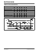
MCP3204/3208 VDD 10 µF 4.096V Reference 0.1 µF 1 µF MCP1541 1 µF IN+ VREF MCP3204 VIN R1 C1 MCP601 IN- + R2 - C2 R3 R4 FIGURE 6-3: The MCP601 Operational Amplifier is used to implement a second order anti-aliasing filter for the signal being converted by the MCP3204. 6.4 Layout Considerations VDD When laying out a printed circuit board for use with analog components, care should be taken to reduce noise wherever possible.
MCP3204/3208 6.5 Utilizing the Digital and Analog Ground Pins The MCP3204/3208 devices provide both digital and analog ground connections to provide another means of noise reduction. As shown in Figure 6-5, the analog and digital circuitry is separated internal to the device. This reduces noise from the digital portion of the device being coupled into the analog portion of the device. The two grounds are connected internally through the substrate, which has a resistance of 5 -10Ω.
MCP3204/3208 7.0 PACKAGING INFORMATION 7.1 Package Marking Information 14-Lead PDIP (300 mil) (MCP3204) Example: XXXXXXXXXXXXXX XXXXXXXXXXXXXX YYWWNNN 14-Lead SOIC (150 mil) (MCP3204) XXXXXXXXXXX XXXXXXXXXXX YYWWNNN 14-Lead TSSOP (4.4mm)* (MCP3204) MCP3204-B I/P e3 0819256 Example: MCP3204-B I/SL e3 XXXXXXXI/XXXX 0819256 Example: XXXXXXXX 3204-C YYWW 0819 NNN 256 Legend: XX...
MCP3204/3208 Package Marking Information (Continued) 16-Lead PDIP (300 mil) (MCP3208) Example: XXXXXXXXXXXXXX XXXXXXXXXXXXXX YYWWNNN 16-Lead SOIC (150 mil) (MCP3208) XXXXXXXXXXXXX XXXXXXXXXXXXX YYWWNNN DS21298E-page 26 MCP3208-BI/P e3 0819256 Example: MCP3208-B I/SL e3 XXXXIXXXXXX 0819256 © 2008 Microchip Technology Inc.
MCP3204/3208 3 % & % ! % 4 " ) ' % 4 $ % % " % %% 255))) & &5 4 N NOTE 1 E1 1 3 2 D E A2 A L A1 c b1 b e eB 6 % & 9 & % 7!&( $ 7+8- 7 7 % ; % % 7: 1 + < < 0 , 0 1 % % 0 < < - , , 0 " " 4 ! " % 4 ! " = "% " "
MCP3204/3208 ! " ! ## $% &' !" ( 3 % & % ! % 4 " ) ' % 4 $ % % " % %% 255))) & &5 4 D N E E1 NOTE 1 1 2 3 e h b A2 A α h c φ L A1 β L1 6 % & 9 & % 7!&( $ 99 - - 7 7 7: ; % : 8 % < < 0 < < < 0 " " 4 4 % " $$ * 1 + : = "% - " " 4 = "% - , 1 +
MCP3204/3208 3 % & % ! % 4 " ) ' % 4 $ % % " % %% 255))) & &5 4 © 2008 Microchip Technology Inc.
MCP3204/3208 )* !*# + ! " !) & )!!" 3 % & % ! % 4 " ) ' % 4 $ % % " % %% 255))) & &5 4 D N E E1 NOTE 1 1 2 e b A2 A c A1 φ L L1 6 % & 9 & % 7!&( $ 99 - - 7 7 7: ; % : 8 % < < > 0 0 < 0 " " 4 4 % " $$ ?0 1 + : = "% - " " 4 = "% - ,
MCP3204/3208 , 3 % & % ! % 4 " ) ' % 4 $ % % " % %% 255))) & &5 4 N NOTE 1 E1 1 2 3 D E A A2 L A1 c b1 e b eB 6 % & 9 & % 7!&( $ 7+8- 7 7 % ; ? % % 7: 1 + < < 0 , 0 1 % % 0 < < - , , 0 " " 4 ! " % 4 ! " = "% " "
MCP3204/3208 , ! " ! ## $% &' !" ( 3 % & % ! % 4 " ) ' % 4 $ % % " % %% 255))) & &5 4 D N E E1 NOTE 1 1 3 2 e b h α h c φ A2 A L β A1 L1 6 % & 9 & % 7!&( $ 99 - - 7 7 7: ; ? % : 8 % < < 0 < < < 0 " " 4 4 % " $$ * 1 + : = "% - " " 4 = "% - , 1 + :
MCP3204/3208 3 % & % ! % 4 " ) ' % 4 $ % % " % %% 255))) & &5 4 © 2008 Microchip Technology Inc.
MCP3204/3208 NOTES: DS21298E-page 34 © 2008 Microchip Technology Inc.
MCP3204/3208 APPENDIX A: REVISION HISTORY Revision E (September 2008) The following is the list of modifications: 1. Updated package outline drawings Section 7.0 “Packaging Information”. in Revision D (January 2007) The following is the list of modifications: 1. Undocumented changes Revision C (May 2002) The following is the list of modifications: 1. Undocumented changes Revision B (August 1999) The following is the list of modifications: 1.
MCP3204/3208 NOTES: DS21298E-page 36 © 2008 Microchip Technology Inc.
MCP3204/3208 PRODUCT IDENTIFICATION SYSTEM To order or obtain information, e.g., on pricing or delivery, refer to the factory or the listed sales office. PART NO.
MCP3204/3208 NOTES: DS21298E-page 38 © 2008 Microchip Technology Inc.
Note the following details of the code protection feature on Microchip devices: • Microchip products meet the specification contained in their particular Microchip Data Sheet. • Microchip believes that its family of products is one of the most secure families of its kind on the market today, when used in the intended manner and under normal conditions. • There are dishonest and possibly illegal methods used to breach the code protection feature.
WORLDWIDE SALES AND SERVICE AMERICAS ASIA/PACIFIC ASIA/PACIFIC EUROPE Corporate Office 2355 West Chandler Blvd. Chandler, AZ 85224-6199 Tel: 480-792-7200 Fax: 480-792-7277 Technical Support: http://support.microchip.com Web Address: www.microchip.