MCP3302/04 13-Bit Differential Input, Low Power A/D Converter with SPI Serial Interface Features General Description • • • • • • • • • • • • • The MCP3302/04 13-bit A/D converter features full differential inputs and low-power consumption in a small package that is ideal for battery-powered systems and remote data acquisition applications.
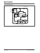
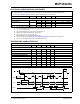
MCP3302/04 Functional Block Diagram VREF CH0 CH1 VDD AGND DGND Input Channel Mux CH7* CDAC Sample & Hold Circuits - Comparator 13-Bit SAR + Control Logic CS/SHDN DIN CLK Shift Register DOUT * Channels 5-7 available on MCP3304 Only DS21697F-page 2 2011 Microchip Technology Inc.
MCP3302/04 1.0 ELECTRICAL CHARACTERISTICS † Notice: Stresses above those listed under “Maximum ratings” may cause permanent damage to the device. This is a stress rating only and functional operation of the device at those or any other conditions above those indicated in the operational listings of this specification is not implied. Exposure to maximum rating conditions for extended periods may affect device reliability. Absolute Maximum Ratings † VDD......................................................
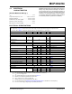
MCP3302/04 ELECTRICAL SPECIFICATIONS (CONTINUED) Electrical Characteristics: Unless otherwise noted, all parameters apply at VDD = 5V, VSS = 0V, and VREF = 5V. Full differential input configuration (Figure 1-5) with fixed common mode voltage of 2.5V. All parameters apply over temperature with TA = -40°C to +85°C (Note 7). Conversion speed (FSAMPLE) is 100 ksps with FCLK = 21*FSAMPLE Parameter Symbol Min Full Scale Input Span CH0 - CH7 -VREF Absolute Input Voltage CH0 - CH7 -0.
MCP3302/04 ELECTRICAL SPECIFICATIONS (CONTINUED) Electrical Characteristics: Unless otherwise noted, all parameters apply at VDD = 5V, VSS = 0V, and VREF = 5V. Full differential input configuration (Figure 1-5) with fixed common mode voltage of 2.5V. All parameters apply over temperature with TA = -40°C to +85°C (Note 7). Conversion speed (FSAMPLE) is 100 ksps with FCLK = 21*FSAMPLE Parameter Symbol Min Typ Max Units Conditions Operating Voltage VDD 4.5 — 5.
MCP3302/04 1.1 Test Circuits VREF = 5V 1 µF MCP330X 1.4V 3 kΩ DOUT IN(+) CL = 100 pF 0.1 µF 0.1 µF 5VP-P Test Point VREFVDD MCP330X IN(-) 5VP-P FIGURE 1-2: VDD = 5V VSS Load Circuit for TR, TF, TDO. VCM = 2.5V Test Point MCP330X VDD VDD/2 3 kΩ DOUT 100 pF TDIS Waveform 2 FIGURE 1-5: Full Differential Test Configuration Example. TEN Waveform TDIS Waveform 1 VSS VREF = 2.5V VDD = 5V 1µF 0.1µF 0.
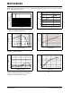
MCP3302/04 2.0 TYPICAL PERFORMANCE CURVES Note: The graphs and tables provided following this note are a statistical summary based on a limited number of samples and are provided for informational purposes only. The performance characteristics listed herein are not tested or guaranteed. In some graphs or tables, the data presented may be outside the specified operating range (e.g., outside specified power supply range) and therefore outside the warranted range.
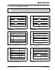
MCP3302/04 Note: Unless otherwise indicated, VDD = VREF = 5V, Full differential input configuration, VSS = 0V, FSAMPLE = 100 ksps, FCLK = 21*FSAMPLE, TA = +25°C. 1 20 0.8 18 0.6 16 2IIVHW (UURU /6% DNL (LSB) 0.4 14 0.2 12 0 10 -0.2 -0.4 8 6 -0.6 4 -0.8 2 -1 -4096 0 -3072 -2048 -1024 0 1024 2048 3072 4096 0 1 2 Code 3 4 5 6 VREF(V) FIGURE 2-7: Differential Nonlinearity (DNL) vs. Code (Representative Part). Offset Error vs. VREF. FIGURE 2-10: 1 0 0.8 DNL (LSB) 0.
MCP3302/04 Note: Unless otherwise indicated, VDD = VREF = 5V, Full differential input configuration, VSS = 0V, FSAMPLE = 100 ksps, FCLK = 21*FSAMPLE, TA = +25°C. 0 80 -10 70 -20 60 SINAD (dB) THD (dB) -30 -40 -50 -60 50 40 30 -70 70 20 -80 10 -90 0 -100 1 10 -40 100 -30 Input Frequency (kHz) FIGURE 2-13: Total Harmonic Distortion (THD) vs. Input Frequency. -10 0 FIGURE 2-16: Signal-to-Noise and Distortion (SINAD) vs. Input Signal Level. 3.1 13 3 12 2.
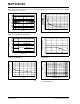
MCP3302/04 450 0 -10 -20 -30 -40 -50 -60 -70 -80 -90 -100 -110 -120 -130 -140 -150 400 350 300 IDD (µA) Amplitude (dB) Note: Unless otherwise indicated, VDD = VREF = 5V, Full differential input configuration, VSS = 0V, FSAMPLE = 100 ksps, FCLK = 21*FSAMPLE, TA = +25°C. 200 150 100 50 0 0 10000 20000 30000 Frequency (Hz) 40000 2 50000 FIGURE 2-19: Frequency Spectrum of 10 kHz Input (Representative Part). 2.5 3 3.5 4 4.5 5 5.5 6 VDD (V) IDD vs. VDD. FIGURE 2-22: 12.85 600 500 12.
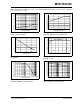
MCP3302/04 Note: Unless otherwise indicated, VDD = VREF = 5V, Full differential input configuration, VSS = 0V, FSAMPLE = 100 ksps, FCLK = 21*FSAMPLE, TA = +25°C. 120 80 100 70 60 IDDS (pA) IREF (µA) 80 60 40 50 40 30 20 20 10 0 0 2 2.5 3 3.5 4 4.5 5 5.5 2 6 2.5 3 3.5 VDD (V) FIGURE 2-25: 4 4.5 5 5.5 6 VDD (V) IREF vs. VDD. FIGURE 2-28: IDDS vs. VDD. 100 120 100 10 IDDS (nA) IREF (µA) 80 60 1 0.1 40 0.01 20 0.001 0 0 50 100 150 -50 200 -25 0 IREF vs.
MCP3302/04 2 80 1.5 79 Common Mode Rejection Ration(dB) Nega ative Gain Error (LSB) Note: Unless otherwise indicated, VDD = VREF = 5V, Full differential input configuration, VSS = 0V, FSAMPLE = 100 ksps, FCLK = 21*FSAMPLE, TA = +25°C. 1 0.5 0 -0.5 -1 -1.5 -2 -50 0 50 100 150 78 77 76 75 74 73 72 71 70 1 Temperature (°C) FIGURE 2-31: Temperature. DS21697F-page 12 Negative Gain Error vs. FIGURE 2-32: vs. Frequency.
MCP3302/04 3.0 PIN DESCRIPTIONS The descriptions of the pins are listed in Table 3-1. TABLE 3-1: PIN FUNCTION TABLE MCP3302 MCP3304 PDIP, SOIC, TSSOP PDIP, SOIC 1 1 CH0 Analog Input 2 2 CH1 Analog Input 3 3 CH2 Analog Input 3.
MCP3302/04 3.7 Analog Ground (AGND) Ground connection to internal analog circuitry. To ensure accuracy, this pin must be connected to the same ground as DGND. If an analog ground plane is available, it is recommended that this device be tied to the analog ground plane in the circuit. See Section 5.6 “Layout Considerations” for more information regarding circuit layout. 3.8 3.9 Power Supply (VDD) The device can operate from 2.7V to 5.5V, but the data conversion performance is from 4.5V to 5.
MCP3302/04 4.0 DEFINITION OF TERMS Bipolar Operation - This applies to either a differential or single-ended input configuration, where both positive and negative codes are output from the A/D converter. Full bipolar range includes all 8192 codes. For bipolar operation on a single-ended input signal, the A/D converter must be configured to operate in pseudo differential mode.
MCP3302/04 NOTES: DS21697F-page 16 2011 Microchip Technology Inc.
MCP3302/04 5.0 APPLICATIONS INFORMATION 5.2 5.1 Conversion Description The analog input of the MCP3302/04 is easily driven, either differentially or single ended. Any signal that is common to the two input channels will be rejected by the common mode rejection of the device. During the charging time of the sample capacitor, a small charging current will be required. For low-source impedances, this input can be driven directly.
MCP3302/04 VDD RS VT = 0.6V CHx CPIN 7 pF VA Sampling Switch VT = 0.6V SS RSS = 1 k CSAMPLE = DAC capacitance = 25 pF ILEAKAGE ±1 nA VSS Legend VA RS CHx CPIN VT ILEAKAGE SS RSS CSAMPLE = = = = = = = = = FIGURE 5-3: 5.2.1 signal source source impedance input channel pad input pin capacitance threshold voltage leakage current at the pindue to various junctions sampling switch sampling switch resistor sample/hold capacitance Analog Input Model.
MCP3302/04 Using an external operation amplifier on the input allows for gain and also buffers the input signal from the input to the ADC allowing for a higher source impedance. This circuit is shown in Figure 5-5. VDD = 5V 10 k 1 k VIN 0.1 µF MCP6021 1 µF + IN+ IN- 1 M MCP330X VREF 5.4 Common Mode Input Range The common mode input range has no restriction and is equal to the absolute input voltage range: VSS -0.3V to VDD + 0.3V.
MCP3302/04 5.5 Buffering/Filtering the Analog Inputs Inaccurate conversion results may occur if the signal source for the A/D converter is not a low-impedance source. Buffering the input will overcome the impedance issue. It is also recommended that an analog filter be used to eliminate any signals that may be aliased back into the conversion results. This is illustrated in Figure 5-9, where an op amp is used to drive the analog input of the MCP3302/04.
MCP3302/04 5.7 Utilizing the Digital and Analog Ground Pins The MCP3302/04 devices provide both digital and analog ground connections to provide another means of noise reduction. As shown in Figure 5-11, the analog and digital circuitry are separated internal to the device. This reduces noise from the digital portion of the device being coupled into the analog portion of the device. The two grounds are connected internally through the substrate which has a resistance of 5 -10Ω.
MCP3302/04 NOTES: DS21697F-page 22 2011 Microchip Technology Inc.
MCP3302/04 6.0 SERIAL COMMUNICATIONS 6.1 Output Code Format The output code format is a binary two’s complement scheme, with a leading sign bit that indicates the sign of the output. If the IN+ input is higher than the INinput, the sign bit will be a zero. If the IN- input is higher, the sign bit will be a ‘1’. The diagram shown in Figure 6-1 shows the output code transfer function. In this diagram, the horizontal axis is the analog input voltage and the vertical axis is the output code of the ADC.
MCP3302/04 Output Code Positive Full Scale Output = VREF -1 LSB 0 + 1111 1111 1111 (+4095) 0 + 1111 1111 1110 (+4094) 0 + 0000 0000 0011 (+3) 0 + 0000 0000 0010 (+2) 0 + 0000 0000 0001 (+1) IN+ > IN- 0 + 0000 0000 0000 (0) IN+ < IN- -VREF 1 + 1111 1111 1111 (-1) 1 + 1111 1111 1110 (-2) Analog Input Voltage IN+ - IN- VREF 1 + 1111 1111 1101 (-3) 1 + 0000 0000 0001 (-4095) Negative Full Scale Output = -VREF FIGURE 6-1: 6.2 1 + 0000 0000 0000 (-4096) Output Code Transfer Function.
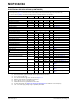
MCP3302/04 TABLE 6-1: CONFIGURATION BITS FOR THE MCP3302 Control Bit Selections Single D2* D1 /Diff D0 Input Configuration Channel Selection TABLE 6-2: CONFIGURATION BITS FOR THE MCP3304 Control Bit Selections Single /Diff D2 D1 D0 Input Configuration Channel Selection 1 X 0 0 single ended CH0 1 0 0 0 single ended CH0 1 X 0 1 single ended CH1 1 0 0 1 single ended CH1 1 X 1 0 single ended CH2 1 0 1 0 single ended CH2 1 X 1 1 single ended CH3 1 0 1 1
MCP3302/04 TSAMPLE TSAMPLE TCSH CS TSUCS CLK Start SGL/ D2 D1 D0 DIFF DIN HI-Z DOUT Start SGL/ DIFF Don’t Care Null SB† B11 B10 B9 B8 B7 B6 B5 B4 B3 B2 B1 B0 * Bit D2 HI-Z TCONV TACQ TDATA ** * After completing the data transfer, if further clocks are applied with CS low, the A/D Converter will output LSB first data, followed by zeros indefinitely. See Figure 6-3 below.
MCP3302/04 6.3 Using the MCP3302/04 with Microcontroller (MCU) SPI Ports As shown in Figure 6-4, the first byte transmitted to the A/D Converter contains 6 leading zeros before the start bit. Arranging the leading zeros this way produces the 13 data bits to fall in positions easily manipulated by the MCU. The sign bit is clocked out of the A/D Converter on the falling edge of clock number 11, followed by the remaining data bits (MSB first).
MCP3302/04 CS SCLK MCU latches data from A/D Converter on rising edges of SCLK 1 2 3 4 5 6 7 8 9 10 11 12 13 14 15 16 17 18 19 20 21 22 23 24 Data is clocked out of A/D Converter on falling edges Start DIN D1 Don’tCare Care Don’t D0 NULL SB B11 B10 B9 BIT B8 B7 B6 B5 B4 B3 B2 B1 B0 X X X X X X X X Start Bit MCU Transmitted Data (Aligned with falling 0 edge of clock) ? = Unknown Bits X = Don’t Care Bits D2 HI-Z DOUT MCU Received Data (Aligned with rising
MCP3302/04 7.0 PACKAGING INFORMATION 7.1 Package Marking Information 14-Lead PDIP (300 mil) Example: XXXXXXXXXXXXXX XXXXXXXXXXXXXX YYWWNNN 14-Lead SOIC (150 mil) MCP3302-B I/P^^ e3 1112256 Example: XXXXXXXXXXX XXXXXXXXXXX YYWWNNN 14-Lead TSSOP (4.4mm) XXXXXXXX XYWW NNN Legend: XX...
MCP3302/04 7.2 Package Marking Information (Continued) 16-Lead PDIP (300 mil) Example: XXXXXXXXXXXXXX XXXXXXXXXXXXXX YYWWNNN 16-Lead SOIC (150 mil) XXXXXXXXXXXXX XXXXXXXXXXXXX YYWWNNN DS21697F-page 30 MCP3304-B I/P e3 1112256 Example: MCP3304-B XXXIIXXXXXXX I/SL e3 1112256 2011 Microchip Technology Inc.
MCP3302/04 3 % & % ! % 4 " ) ' % 4 $ % % " % %% 255))) & &5 4 N NOTE 1 E1 1 3 2 D E A2 A L A1 c b1 b e eB 6 % & 9 & % 7!&( $ 7+8- 7 7 % ; % % 7: 1 + < < 0 , 0 1 % % 0 < < - , , 0 " " 4 ! " % 4 ! " = "% " "
MCP3302/04 Note: For the most current package drawings, please see the Microchip Packaging Specification located at http://www.microchip.com/packaging DS21697F-page 32 2011 Microchip Technology Inc.
MCP3302/04 Note: For the most current package drawings, please see the Microchip Packaging Specification located at http://www.microchip.com/packaging 2011 Microchip Technology Inc.
MCP3302/04 3 % & % ! % 4 " ) ' % 4 $ % % " % %% 255))) & &5 4 DS21697F-page 34 2011 Microchip Technology Inc.
MCP3302/04 Note: For the most current package drawings, please see the Microchip Packaging Specification located at http://www.microchip.com/packaging 2011 Microchip Technology Inc.
MCP3302/04 Note: For the most current package drawings, please see the Microchip Packaging Specification located at http://www.microchip.com/packaging DS21697F-page 36 2011 Microchip Technology Inc.
MCP3302/04 Note: For the most current package drawings, please see the Microchip Packaging Specification located at http://www.microchip.com/packaging 2011 Microchip Technology Inc.
MCP3302/04 ! 3 % & % ! % 4 " ) ' % 4 $ % % " % %% 255))) & &5 4 N NOTE 1 E1 1 2 3 D E A A2 L A1 c b1 e b eB 6 % & 9 & % 7!&( $ 7+8- 7 7 % ; ? % % 7: 1 + < < 0 , 0 1 % % 0 < < - , , 0 " " 4 ! " % 4 ! " = "% " "
MCP3302/04 Note: For the most current package drawings, please see the Microchip Packaging Specification located at http://www.microchip.com/packaging 2011 Microchip Technology Inc.
MCP3302/04 Note: For the most current package drawings, please see the Microchip Packaging Specification located at http://www.microchip.com/packaging DS21697F-page 40 2011 Microchip Technology Inc.
MCP3302/04 Note: For the most current package drawings, please see the Microchip Packaging Specification located at http://www.microchip.com/packaging 2011 Microchip Technology Inc.
MCP3302/04 NOTES: DS21697F-page 42 2011 Microchip Technology Inc.
MCP3302/04 APPENDIX A: REVISION HISTORY Revision F (April 2011) The following is the list of modifications: 1. 2. Updated content to designate that the devices now have tested specifications in the 4.5V to 5.5V supply range. Removed figures 2.4 to 2.6, 2.10 to 2.12, 2.16 and 2.17 in Section 2.0 “Typical Performance Curves”. Revision E (December 2008) The following is the list of modifications: Update to Package Outline Drawings.
MCP3302/04 NOTES: DS21697F-page 44 2011 Microchip Technology Inc.
MCP3302/04 PRODUCT IDENTIFICATION SYSTEM To order or obtain information, e.g., on pricing or delivery, contact the local Microchip sales office. PART NO.
MCP3302/04 NOTES: DS21697F-page 46 2011 Microchip Technology Inc.
Note the following details of the code protection feature on Microchip devices: • Microchip products meet the specification contained in their particular Microchip Data Sheet. • Microchip believes that its family of products is one of the most secure families of its kind on the market today, when used in the intended manner and under normal conditions. • There are dishonest and possibly illegal methods used to breach the code protection feature.
Worldwide Sales and Service AMERICAS Corporate Office 2355 West Chandler Blvd. Chandler, AZ 85224-6199 Tel: 480-792-7200 Fax: 480-792-7277 Technical Support: http://www.microchip.com/ support Web Address: www.microchip.