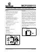
MCP3550/1/3 Low-Power, Single-Channel 22-Bit Delta-Sigma ADCs Features Description • 22-bit ADC in Small 8-pin MSOP Package with Automatic Internal Offset and Gain Calibration • Low-Output Noise of 2.5 µVRMS with Effective Resolution of 21.
MCP3550/1/3 NOTES: DS21950E-page 2 © 2009 Microchip Technology Inc.
MCP3550/1/3 1.0 ELECTRICAL CHARACTERISTICS 1.1 Maximum Ratings* † Notice: Stresses above those listed under "Maximum Ratings" may cause permanent damage to the device. This is a stress rating only and functional operation of the device at those or any other conditions above those indicated in the operation listings of this specification is not implied. Exposure to maximum rating conditions for extended periods may affect device reliability. VDD...........................................................
MCP3550/1/3 DC CHARACTERISTICS (CONTINUED) Electrical Specifications: Unless otherwise indicated, all parameters apply at -40°C ≤ TA ≤ +85°C, VDD = 2.7V or 5.0V. VREF = 2.5V. VIN+ = VIN- = VCM = VREF/2. All ppm units use 2*VREF as full scale range. Unless otherwise noted, specification applies to entire MCP3550/1/3 family.
MCP3550/1/3 DC CHARACTERISTICS (CONTINUED) Electrical Specifications: Unless otherwise indicated, all parameters apply at -40°C ≤ TA ≤ +85°C, VDD = 2.7V or 5.0V. VREF = 2.5V. VIN+ = VIN- = VCM = VREF/2. All ppm units use 2*VREF as full scale range. Unless otherwise noted, specification applies to entire MCP3550/1/3 family. Parameters Voltage Output Low (SDO/RDY) Input leakage Current (CS, SCK) Internal Pin Capacitance (CS, SCK, SDO/RDY) Note 1: 2: 3: 4: 5: 6: Sym Min Typ Max Units VOL — — 0.
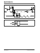
MCP3550/1/3 tRDY tCSHSD tCSD CS tCSL tDIS SDO /RDY tDO tHI tSU SCK FIGURE 1-1: fSCK tLO Serial Timing. VDD tPUCSL CS FIGURE 1-2: DS21950E-page 6 Power-up Timing. © 2009 Microchip Technology Inc.
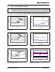
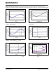
MCP3550/1/3 2.0 TYPICAL PERFORMANCE CURVES Note: The graphs and tables provided following this note are a statistical summary based on a limited number of samples and are provided for informational purposes only. The performance characteristics listed herein are not tested or guaranteed. In some graphs or tables, the data presented may be outside the specified operating range (e.g., outside specified power supply range) and therefore outside the warranted range. 5 4 3 2 1 0 -1 -2 -3 -4 -5 -2.
MCP3550/1/3 Note: Unless otherwise specified, TA = +25°C, VDD = 5V, VREF = 2.5V, VSS = 0V, VCM = VREF/2, VIN+ = VIN-. All ppm units use 2*VREF as full scale range. Unless otherwise noted, graphs apply to entire MCP3550/1/3 family. Output Noise (µVRMS ) Output Noise (µV RMS) 15 10 MCP3553 5 MCP3550/1 0 -2.5 -1.5 -0.5 0.5 1.5 2.5 10 9 8 7 6 5 4 3 2 1 0 MCP3553 MCP3550/1 -50 VIN (V) -25 0 FIGURE 2-10: Temperature. FIGURE 2-7: Output Noise vs. Input Voltage (VDD = 5.0V).
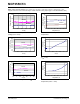
MCP3550/1/3 4000 5 4 3 2 1 0 -1 -2 -3 -4 -5 Number of Occurrences Full Scale Error (ppm) Note: Unless otherwise specified, TA = +25°C, VDD = 5V, VREF = 2.5V, VSS = 0V, VCM = VREF/2, VIN+ = VIN-. All ppm units are ratioed against 2*VREF . Unless otherwise noted, graphs apply to entire MCP3550/1/3 family. Positive Full Scale Negative Full Scale VDD = 5V VREF = 2.5V VCM = 1.25V VIN = 0V TA = 25C 16384 consecutiv e readings 3500 3000 2500 2000 1500 1000 500 0 2.5 3 3.5 4 4.5 5 5.
MCP3550/1/3 5 4 3 2 1 0 -1 -2 -3 -4 -5 -2.5 6 Maximum TUE (ppm) TUE (ppm) Note: Unless otherwise specified, TA = +25°C, VDD = 5V, VREF = 2.5V, VSS = 0V, VCM = VREF/2, VIN+ = VIN-. All ppm units use 2*VREF as full scale range. Unless otherwise noted, graphs apply to entire MCP3550/1/3 family. -1.5 -1 -0.5 0 0.5 VIN (V) 1 1.5 2 3 2 1 -50 2.5 -3 -2 -1 0 1 0 FIGURE 2-22: Temperature. 10 8 6 4 2 0 -2 -4 -6 -8 -10 -4 -25 50 75 100 125 2 3 4 5 Maximum TUE vs. 5 4.5 4 3.5 3 2.5 2 1.
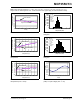
MCP3550/1/3 160 200 180 160 140 120 100 80 60 40 20 0 140 MCP3550-60, MCP3553 MCP3550-50, MCP3550/1 120 MCP3550-60, MCP3553 IDD (µA) IDD (µA) Note: Unless otherwise specified, TA = +25°C, VDD = 5V, VREF = 2.5V, VSS = 0V, VCM = VREF/2, VIN+ = VIN-. All ppm units use 2*VREF as full scale range. Unless otherwise noted, graphs apply to entire MCP3550/1/3 family. MCP3550-50, MCP3550/1 100 80 60 40 20 0 2.5 3 3.5 4 4.5 5 5.5 -50 -25 VDD (V) FIGURE 2-25: IDD vs. VDD.
MCP3550/1/3 NOTES: DS21950E-page 12 © 2009 Microchip Technology Inc.
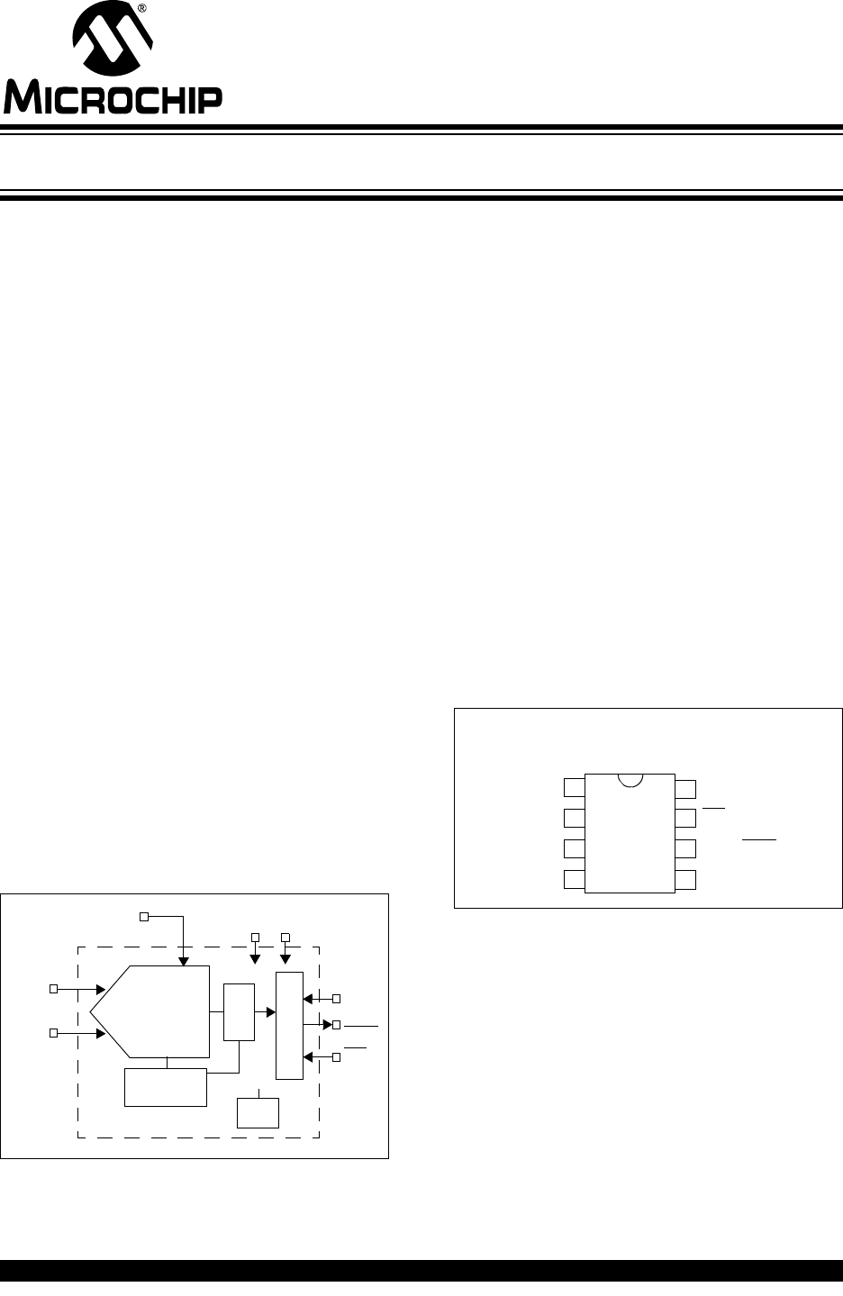
MCP3550/1/3 3.0 PIN DESCRIPTIONS The descriptions of the pins are listed in Table 3-1.
MCP3550/1/3 3.6 Chip Select (CS) CS gates all communication to the device and can be used to select multiple devices that share the same SCK and SDO/RDY pins. This pin is also used to control the internal conversions, which begin on the falling edge of CS. Raising CS before the first internal conversion is complete places the device in Single Conversion mode. Leaving CS low will place the device in Continuous Conversion mode (i.e., additional internal conversions will automatically occur).
MCP3550/1/3 4.0 DEVICE OVERVIEW The MCP3550/1/3 devices communicate with a simple 3-wire SPI interface. The interface controls the conversion start event, with an added feature of an auto-conversion at system power-up by tying the CS pin to logic-low. The device can communicate with bus speeds of up to 5 MHz, with 50 pF capacitive loading. The interface offers two conversion modes: Single Conversion mode for multiplexed applications and a Continuous Conversion mode for multiple conversions in series.
MCP3550/1/3 4.1 MCP3550/1/3 Delta-Sigma Modulator with Internal Offset and Gain Calibration 4.2 The MCP3550/1/3 devices include a digital decimation filter, which is a fourth-order modified SINC filter. This filter averages the incoming bit stream from the modulator and outputs a 22-bit conversion word in binary two's complement.
MCP3550/1/3 0 0 -20 -20 Normal Mode Rejection (dB) Attenuation (dB) : -40 -60 -80 -100 -40 -60 -80 -100 -120 -120 0 50 100 150 200 -140 0 Frequency (Hz) 28160 56320 84480 112640 140800 168960 197120 225280 253440 Frequency (Hz) FIGURE 4-5: SINC Filter Response at Integer Multiples of the Sampling Frequency (fs). FIGURE 4-2: SINC Filter Response, MCP3550-50 Device. : 4.
MCP3550/1/3 4.4 Differential Analog Inputs The MCP3550/1/3 devices accept a fully differential analog input voltage to be connected to the VIN+ and VIN- input pins. The differential voltage that is converted is defined by VIN = VIN+ – VIN-. The differential voltage range specified for ensured accuracy is from -VREF to +VREF. The converter will output valid and usable codes from -112% to 112% of output range (see Section 5.0 “Serial Interface”) at room temperature.
MCP3550/1/3 Once a power-up event has occurred, the device must require additional time before a conversion can take place. During this time, all internal analog circuitry must settle before the first conversion can occur. An internal timer counts 32 internal clock periods before the internal oscillator can provide clock to the conversion process. This allows all internal analog circuitry to settle to their proper operating point.
MCP3550/1/3 NOTES: DS21950E-page 20 © 2009 Microchip Technology Inc.
MCP3550/1/3 5.0 SERIAL INTERFACE 5.1 Overview Serial communication between the microcontroller and the MCP3550/1/3 devices is achieved using CS, SCK and SDO/RDY. There are two modes of operation: Single Conversion and Continuous Conversion. CS controls the conversion start. There are 24 bits in the data word: 22 bits of conversion data and two overflow bits. The conversion process takes place via the internal oscillator and the status of this conversion must be detected.
MCP3550/1/3 5.2 Controlling Internal Conversions and the Internal Oscillator During Shutdown mode, on the falling edge of CS, the conversion process begins. During this process, the internal oscillator clocks the delta-sigma modulator and the SINC filter until a conversion is complete. This conversion time is tCONV and the timing is shown in Figure 5-2. At the end of tCONV, the digital filter has settled completely and there is no latency involved with the digital SINC filter of the MCP3550/1/3.
MCP3550/1/3 5.3 Single Conversion Mode If a rising edge of Chip Select (CS) occurs during tCONV, a subsequent conversion will not take place and the device will enter low-power Shutdown mode after tCONV completes. This is referred to as Single Conversion mode. This operation is demonstrated in Figure 5-2. Note that a falling edge of CS during the same conversion that detected a rising edge, as in Figure 5-2, will not initiate a new conversion.
MCP3550/1/3 5.4.1 READY FUNCTION OF SDO/RDY PIN IN CONTINUOUS CONVERSION MODE The device enters Continuous Conversion mode if no rising edge of CS is seen during tCONV and consecutive conversions ensue. SDO/RDY will be high, indicating that a conversion is in process. When a conversion is complete, SDO/RDY will change to a Low state. With the Low state of SDO/RDY after this first conversion, the conversion data can be accessed with the combination of SCK and SDO/RDY.
MCP3550/1/3 5.5 Using The MCP3550/1/3 with Microcontroller (MCU) SPI Ports It is required that the microcontroller SPI port be configured to clock out data on the falling edge of clock and latch data in on the rising edge. Figure 5-6 depicts the operation shown in SPI mode 1,1, which requires that the SCK from the MCU idles in the High state, while Figure 5-7 shows the similar case of SPI Mode 0,0, where the clock idles in the Low state.
MCP3550/1/3 NOTES: DS21950E-page 26 © 2009 Microchip Technology Inc.
MCP3550/1/3 6.0 PACKAGING INFORMATION 6.1 Package Marking Information Example: 8-Lead MSOP XXXXXX 3553E YWWNNN 951256 8-Lead SOIC (150 mil) XXXXXXXX XXXXYYWW NNN Example (MCP3550): 3550-50E e3 0951 SN^^ 256 Example (MCP3551): MCP3551E e3 0951 SN^^ 256 Legend: XX...
MCP3550/1/3 1 % & % ! % 2 " ) ' % 2 $ % % " % %% 033))) & &3 2 D N E E1 NOTE 1 1 2 e b A2 A c φ L L1 A1 4 % & 5 & % 6!&( $ 55 * * 6 6 67 8 9 % 7 ; % < < + 9+ + < + " " 2 2 % " $$ :+ . / 7 = "% * " " 2 = "% * , .
MCP3550/1/3 ! "#$% & ' () 1 % & % ! % 2 " ) ' % 2 $ % % " % %% 033))) & &3 2 D e N E E1 NOTE 1 1 2 3 α h b h A2 A c φ L A1 L1 4 % & 5 & % 6!&( $ β 55 * * 6 6 67 8 9 % 7 ; % < < + < < < + " " 2 2 % " $$ ? . / + 7 = "% * " " 2 = "% * , .
MCP3550/1/3 ! "#$% & ' () 1 % & % ! % 2 " ) ' % 2 $ % % " % %% 033))) & &3 2 DS21950E-page 30 © 2009 Microchip Technology Inc.
MCP3550/1/3 APPENDIX A: REVISION HISTORY Revision E (April 2009) The following is the list of modifications: 1. 2. 3. Numerous changes made throughout document. Too numerous to itemize. DC Characteristics Table, Conversion Times: Changed all minimums from -1.0% to -2.0%. Changed typical for MCP3551 from 72.73 to 73.1. Changed all maximums from +1.0% to +2.0%. Packaging Outline drawings updated..
MCP3550/1/3 NOTES: DS21950E-page 32 © 2009 Microchip Technology Inc.
MCP3550/1/3 PRODUCT IDENTIFICATION SYSTEM To order or obtain information, e.g., on pricing or delivery, refer to the factory or the listed sales office. Device: PART NO.
MCP3550/1/3 NOTES: DS21950E-page 34 © 2009 Microchip Technology Inc.
Note the following details of the code protection feature on Microchip devices: • Microchip products meet the specification contained in their particular Microchip Data Sheet. • Microchip believes that its family of products is one of the most secure families of its kind on the market today, when used in the intended manner and under normal conditions. • There are dishonest and possibly illegal methods used to breach the code protection feature.
WORLDWIDE SALES AND SERVICE AMERICAS ASIA/PACIFIC ASIA/PACIFIC EUROPE Corporate Office 2355 West Chandler Blvd. Chandler, AZ 85224-6199 Tel: 480-792-7200 Fax: 480-792-7277 Technical Support: http://support.microchip.com Web Address: www.microchip.