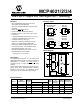
MCP4021/2/3/4 Low-Cost NV Digital POT with WiperLock™ Technology Package Types • Non-volatile Digital Potentiometer in SOT-23, SOIC, MSOP and DFN packages • 64 Taps: 63 Resistors with Taps to terminal A and terminal B • Simple Up/Down (U/D) Protocol • Power-on Recall of Saved Wiper Setting • Resistance Values: 2.1 kΩ, 5 kΩ, 10 kΩ or 50 kΩ • Low Tempco: - Absolute (Rheostat): 50 ppm (0°C to 70°C typ.) - Ratiometric (Potentiometer): 10 ppm (typ.) • Low Wiper Resistance: 75Ω (typ.
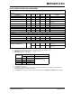
MCP4021/2/3/4 1.0 ELECTRICAL CHARACTERISTICS † Notice: Stresses above those listed under “Maximum Ratings” may cause permanent damage to the device. This is a stress rating only and functional operation of the device at those or any other conditions above those indicated in the operational listings of this specification is not implied. Exposure to maximum rating conditions for extended periods may affect device reliability. Absolute Maximum Ratings † VDD ..................................................
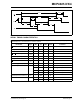
MCP4021/2/3/4 AC/DC CHARACTERISTICS (CONTINUED) Electrical Specifications: Unless otherwise indicated, all parameters apply across the specified operating ranges. TA = -40°C to +125°C, 2.1 kΩ, 5 kΩ, 10 kΩ and 50 kΩ devices. Typical specifications represent values for VDD = 5.5V, VSS = 0V, TA = +25°C.
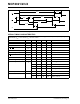
MCP4021/2/3/4 AC/DC CHARACTERISTICS (CONTINUED) Electrical Specifications: Unless otherwise indicated, all parameters apply across the specified operating ranges. TA = -40°C to +125°C, 2.1 kΩ, 5 kΩ, 10 kΩ and 50 kΩ devices. Typical specifications represent values for VDD = 5.5V, VSS = 0V, TA = +25°C.
MCP4021/2/3/4 AC/DC CHARACTERISTICS (CONTINUED) Electrical Specifications: Unless otherwise indicated, all parameters apply across the specified operating ranges. TA = -40°C to +125°C, 2.1 kΩ, 5 kΩ, 10 kΩ and 50 kΩ devices. Typical specifications represent values for VDD = 5.5V, VSS = 0V, TA = +25°C. Parameters Sym Min Typ Max Units VIH 0.7 VDD — — V Conditions Digital Inputs/Outputs (CS, U/D) Input High Voltage VIL — — 0.3 VDD V High-Voltage Input Entry Voltage VIHH 8.5 — 12.
MCP4021/2/3/4 tCSHI tCSLO CS tLUC 1/fUD tLO tLCUF tLUC tLCUF U/D tHI tLCUR tS tS W FIGURE 1-1: Increment Timing Waveform. SERIAL TIMING CHARACTERISTICS Electrical Specifications: Unless otherwise noted, all parameters apply across the specified operating ranges. Extended (E): VDD = +2.7V to 5.5V, TA = -40°C to +125°C.
MCP4021/2/3/4 tCSHI tCSLO CS 1/fUD tLUC tLUC tHI tLCUF U/D tLO tLCUR tS tS W FIGURE 1-2: Decrement Timing Waveform. SERIAL TIMING CHARACTERISTICS Electrical Specifications: Unless otherwise noted, all parameters apply across the specified operating ranges. Extended (E): VDD = +2.7V to 5.5V, TA = -40°C to +125°C.
MCP4021/2/3/4 tCSHI tCSLO 12V CS 5V tHUC 1/fUD tLO tHCUF tHUC tHCUF U/D tHI tHCUR tS tS W FIGURE 1-3: High-Voltage Increment Timing Waveform. SERIAL TIMING CHARACTERISTICS Electrical Specifications: Unless otherwise noted, all parameters apply across the specified operating ranges. Extended (E): VDD = +2.7V to 5.5V, TA = -40°C to +125°C.
MCP4021/2/3/4 tCSHI tCSLO CS 12V 5V 1/fUD tHUC tHUC tHI tHCUF U/D tLO tHCUR tS tS W FIGURE 1-4: High-Voltage Decrement Timing Waveform. SERIAL TIMING CHARACTERISTICS Electrical Specifications: Unless otherwise noted, all parameters apply across the specified operating ranges. Extended (E): VDD = +2.7V to 5.5V, TA = -40°C to +125°C.
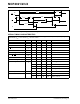
MCP4021/2/3/4 TEMPERATURE CHARACTERISTICS Electrical Specifications: Unless otherwise indicated, VDD = +2.7V to +5.5V, VSS = GND.
MCP4021/2/3/4 2.0 TYPICAL PERFORMANCE CURVES Note: The graphs and tables provided following this note are a statistical summary based on a limited number of samples and are provided for informational purposes only. The performance characteristics listed herein are not tested or guaranteed. In some graphs or tables, the data presented may be outside the specified operating range (e.g., outside specified power supply range) and therefore outside the warranted range. 250 2.7V -40°C 2.7V 25°C 2.7V 85°C 2.
MCP4021/2/3/4 Note: Unless otherwise indicated, TA = +25°C, VDD = 5V, VSS = 0V. INL 100 0.075 120 0.05 100 0.025 80 0 DNL 60 -0.025 40 -0.05 RW 20 -0.1 0 8 25C Rw 25C INL 25C DNL 85C Rw 85C INL 85C DNL 125C Rw 125C INL 125C DNL 300 0 DNL RW 100 -0.05 0 -0.1 0 60 8 16 24 32 40 48 Wiper Setting (decimal) 56 FIGURE 2-7: 2.1 kΩ Pot Mode – RW (Ω), INL (LSb), DNL (LSb) vs. Wiper Setting and Ambient Temperature (VDD = 2.7V). DS21945E-page 12 0.2 40 0 DNL RW -0.2 -0.
MCP4021/2/3/4 Note: Unless otherwise indicated, TA = +25°C, VDD = 5V, VSS = 0V. 2500 -40°C 25°C 85°C 125°C 2000 2060 RWB (Ohms) Nominal Resistance (RAB) (Ohms) 2080 VDD = 5.5V 2040 1500 1000 2020 500 VDD = 2.7V 2000 0 -40 0 40 80 Ambient Temperature (°C) 120 FIGURE 2-10: 2.1 kΩ – Nominal Resistance (Ω) vs. Ambient Temperature and VDD. © 2006 Microchip Technology Inc. 0 8 16 24 32 40 48 Wiper Setting (decimal) 56 64 FIGURE 2-11: 2.1 kΩ – RWB (Ω) vs.
MCP4021/2/3/4 Note: Unless otherwise indicated, TA = +25°C, VDD = 5V, VSS = 0V. WIPER WIPER U/D U/D FIGURE 2-12: 2.1 kΩ – Low-Voltage Decrement Wiper Settling Time (VDD = 2.7V). FIGURE 2-15: 2.1 kΩ – Low-Voltage Increment Wiper Settling Time (VDD = 2.7V). WIPER WIPER U/D U/D FIGURE 2-13: 2.1 kΩ – Low-Voltage Decrement Wiper Settling Time (VDD = 5.5V). FIGURE 2-16: 2.1 kΩ – Low-Voltage Increment Wiper Settling Time (VDD = 5.5V). WIPER VDD FIGURE 2-14: Response Time. DS21945E-page 14 2.
MCP4021/2/3/4 Note: Unless otherwise indicated, TA = +25°C, VDD = 5V, VSS = 0V. 125C Rw 125C INL 125C DNL 0.075 120 0.05 100 0.025 INL 80 0 DNL 60 -0.025 40 -0.05 RW 20 8 16 24 32 40 48 60 0 DNL 40 -0.2 RW -0.4 -0.6 8 85C Rw 85C INL 85C DNL 125C Rw 125C INL 125C DNL 600 0.075 300 0.025 250 0 DNL -0.025 RW 150 24 100 -0.05 50 -40C Rw -40C INL -40C DNL 500 -0.075 400 25C Rw 25C INL 25C DNL 0 -0.
MCP4021/2/3/4 Note: Unless otherwise indicated, TA = +25°C, VDD = 5V, VSS = 0V. 6000 2.7V Vdd 5.5V Vdd 4925 4900 4875 VDD = 5.5V 4850 -40°C 25°C 85°C 125°C 5000 RWB (Ohms) Nominal Resistance (RAB) (Ohms) 4950 4000 3000 2000 1000 4825 VDD = 2.7V 0 4800 -40 -20 0 20 40 60 80 100 120 Ambient Temperature (°C) FIGURE 2-21: 5 kΩ – Nominal Resistance (Ω) vs. Ambient Temperature and VDD. DS21945E-page 16 0 8 16 24 32 40 48 Wiper Setting (decimal) 56 64 FIGURE 2-22: 5 kΩ – RWB (Ω) vs.
MCP4021/2/3/4 Note: Unless otherwise indicated, TA = +25°C, VDD = 5V, VSS = 0V. WIPER WIPER U/D U/D FIGURE 2-23: 5 kΩ – Low-Voltage Decrement Wiper Settling Time (VDD = 2.7V). FIGURE 2-25: 5 kΩ – Low-Voltage Increment Wiper Settling Time (VDD = 2.7V). WIPER WIPER U/D FIGURE 2-24: 5 kΩ – Low-Voltage Decrement Wiper Settling Time (VDD = 5.5V). © 2006 Microchip Technology Inc. U/D FIGURE 2-26: 5 kΩ – Low-Voltage Increment Wiper Settling Time (VDD = 5.5V).
MCP4021/2/3/4 Note: Unless otherwise indicated, TA = +25°C, VDD = 5V, VSS = 0V. 125C Rw 125C INL 125C DNL 0.05 120 0.025 100 DNL 80 0 INL 60 -0.025 40 -0.05 RW 20 -0.075 0 -40C Rw -40C INL -40C DNL 80 25C Rw 25C INL 25C DNL 85C Rw 85C INL 85C DNL 350 125C Rw 125C INL 125C DNL INL 250 -0.025 200 -0.05 150 RW 100 0.05 60 0 40 -0.05 RW -0.1 -0.15 500 0.025 0 300 -0.
MCP4021/2/3/4 12000 10250 10230 10210 10190 10170 10150 10130 10110 10090 10070 10050 -40°C 25°C 85°C 125°C 10000 VDD = 5.5V RWB (Ohms) Nominal Resistance (RAB) (Ohms) Note: Unless otherwise indicated, TA = +25°C, VDD = 5V, VSS = 0V. 8000 6000 4000 2000 VDD = 2.7V 0 -40 -20 0 20 40 60 80 100 120 Ambient Temperature (°C) FIGURE 2-31: 10 kΩ – Nominal Resistance (Ω) vs. Ambient Temperature and VDD. © 2006 Microchip Technology Inc.
MCP4021/2/3/4 Note: Unless otherwise indicated, TA = +25°C, VDD = 5V, VSS = 0V. WIPER WIPER U/D FIGURE 2-33: 10 kΩ – Low-Voltage Decrement Wiper Settling Time (VDD = 2.7V). WIPER U/D FIGURE 2-34: 10 kΩ – Low-Voltage Decrement Wiper Settling Time (VDD = 5.5V). DS21945E-page 20 U/D FIGURE 2-35: 10 kΩ – Low-Voltage Increment Wiper Settling Time (VDD = 2.7V). WIPER U/D FIGURE 2-36: 10 kΩ – Low-Voltage Increment Wiper Settling Time (VDD = 5.5V). © 2006 Microchip Technology Inc.
MCP4021/2/3/4 Note: Unless otherwise indicated, TA = +25°C, VDD = 5V, VSS = 0V. 0.1 125C Rw 125C INL 125C DNL 200 0.05 DNL 120 0 INL 80 -0.05 RW 40 8 16 24 32 40 48 50 -0.1 0 8 125C Rw 125C INL 125C DNL 400 300 600 0.025 500 -0.025 INL 200 -0.05 -0.075 RW 0 -0.1 8 16 24 32 40 48 56 Wiper Setting (decimal) FIGURE 2-38: 50 kΩ Pot Mode – RW (Ω), INL (LSb), DNL (LSb) vs. Wiper Setting and Ambient Temperature (VDD = 2.7V). © 2006 Microchip Technology Inc.
MCP4021/2/3/4 Note: Unless otherwise indicated, TA = +25°C, VDD = 5V, VSS = 0V. 60000 49600 -40C 25C 85C 125C 50000 49400 VDD = 5.5V 49200 49000 48800 VDD = 2.7V 48600 48400 RWB (Ohms) Nominal Resistance (RAB) (Ohms) 49800 40000 30000 20000 10000 48200 48000 0 -40 -20 0 20 40 60 80 100 120 Ambient Temperature (°C) FIGURE 2-41: 50 kΩ – Nominal Resistance (Ω) vs. Ambient Temperature and VDD.
MCP4021/2/3/4 Note: Unless otherwise indicated, TA = +25°C, VDD = 5V, VSS = 0V. U/D U/D WIPER WIPER FIGURE 2-43: 50 kΩ – Low-Voltage Decrement Wiper Settling Time (VDD = 2.7V). FIGURE 2-46: 50 kΩ – Low-Voltage Increment Wiper Settling Time (VDD = 2.7V). U/D U/D WIPER WIPER FIGURE 2-44: 50 kΩ – Low-Voltage Decrement Wiper Settling Time (VDD = 5.5V). FIGURE 2-47: 50 kΩ - Low-Voltage Increment Wiper Settling Time (VDD = 5.5V). WIPER VDD FIGURE 2-45: Response Time.
MCP4021/2/3/4 Note: Unless otherwise indicated, TA = +25°C, VDD = 5V, VSS = 0V. -3dB Frequency (MHz) 4.5 4 A 2.1 k: +5V 3.5 3 VIN 2.5 5 k: 2 1.5 10 k: 1 0.5 W ~ OFFSET GND DUT B + VOUT - 50 k: 2.5V DC 0 -40 25 125 Temperature (°C) FIGURE 2-48: Temperature. DS21945E-page 24 -3 dB Bandwidth vs. FIGURE 2-49: Circuit. -3 dB Bandwidth Test © 2006 Microchip Technology Inc.
MCP4021/2/3/4 3.0 PIN DESCRIPTIONS The descriptions of the pins are listed in Table 3-1.
MCP4021/2/3/4 3.6 Chip Select (CS) The CS pin is the chip select input. Forcing the CS pin to VIL enables the serial commands. These commands can increment and decrement the wiper. Depending on the command, the wiper may (or may not) be saved to non-volatile memeory (EEPROM). Forcing the CS pin to VIHH enables the high-voltage serial commands. These commands can increment and decrement the wiper and enable or disable the WiperLock technology. The wiper is saved to non-volatile memory (EEPROM). 3.
MCP4021/2/3/4 4.0 GENERAL OVERVIEW EQUATION 4-1: The MCP402X devices are general purpose digital potentiometers intended to be used in applications where a programmable resistance with moderate bandwidth is desired. Applications generally suited for the MCP402X devices include: • • • • Set point or offset trimming Sensor calibration Selectable gain and offset amplifier designs Cost-sensitive mechanical trim pot replacement There are 63 resistors in a string between terminal A and terminal B.
MCP4021/2/3/4 serial • Incrementing or decrementing the wiper setting • Writing the wiper setting to the non-volatile memory Enabling and disabling the WiperLock technology feature requires high-voltage serial commands (CS = VIHH). Incrementing and decrementing the wiper requires high-voltage commands when the feature is enabled.
MCP4021/2/3/4 5.0 SERIAL INTERFACE 5.2 5.1 Overview The MCP402X devices support 10 serial commands. The commands can be grouped into the following types: The MCP4021/2/3/4 utilizes a simple 2-wire interface to increment or decrement the digital potentiometer’s wiper terminal (W), store the wiper setting in non-volatile memory and turn the WiperLock technology feature on or off. This interface uses the Chip Select (CS) pin, while the U/D pin is the Up/Down input.
MCP4021/2/3/4 5.2.1 INCREMENT WITHOUT WRITING WIPER SETTING TO EEPROM The EEPROM value has not been updated to this new wiper value, so if the device voltage is lowered below the RAM retention voltage of the device, once the device returns to the operating range, the wiper will be loaded with the wiper setting in the EEPROM. This mode is achieved by initializing the U/D pin to a high state (VIH) prior to achieving a low state (VIL) on the CS pin.
MCP4021/2/3/4 5.2.2 INCREMENT WITH WRITING WIPER SETTING TO EEPROM To ensure that “unexpected” transitions on the U/D pin do not cause the wiper setting to increment, the U/D pin should be driven low and the CS pin forced to VIH as soon as possible (within device specifications) after the last desired increment occurs. This mode is achieved by initializing the U/D pin to a high state (VIH) prior to achieving a low state (VIL) on the CS pin.
MCP4021/2/3/4 5.2.3 DECREMENT WITHOUT WRITING WIPER SETTING TO EEPROM The EEPROM value has not been updated to this new wiper value, so, if the device voltage is lowered below the RAM retention voltage of the device, once the device returns to the operating range, the wiper will be loaded with the wiper setting in the EEPROM. This mode is achieved by initializing the U/D pin to a low state (VIL) prior to achieving a low state (VIL) on the CS pin.
MCP4021/2/3/4 5.2.4 DECREMENT WITH WRITING WIPER SETTING TO EEPROM To ensure that “unexpected” transitions on the U/D pin do not cause the wiper setting to decrement, the U/D pin should be driven low (VIL) and the CS pin forced to VIH as soon as possible (within device specifications) after the last desired increment occurs. This mode is achieved by initializing the U/D pin to a low state (VIL) prior to achieving a low state (VIL) on the CS pin.
MCP4021/2/3/4 5.2.5 WRITE WIPER SETTING TO EEPROM To write the current wiper setting to EEPROM, force both the CS pin and U/D pin to VIH. Then force the CS pin to VIL. Before there is a rising edge on the U/D pin, force the CS pin to VIH. This causes the wiper setting value to be written to EEPROM. Note: After the U/D pin is forced to VIL, each rising edge on the U/D pin will cause the wiper to increment.
MCP4021/2/3/4 5.2.6 HIGH-VOLTAGE INCREMENT AND DISABLE WiperLock TECHNOLOGY After the CS pin is driven to VIH (from VIHH), all other serial commands are ignored until the EEPROM write cycle (tWC) completes. This mode is achieved by initializing the U/D pin to a high state (VIH) prior to the CS pin being driven to VIHH. Subsequent rising edges of the U/D pin increment the wiper setting toward terminal A. Set the U/D pin to the high state (VIH) prior to forcing the CS pin to VIH.
MCP4021/2/3/4 5.2.7 HIGH-VOLTAGE INCREMENT AND ENABLE WiperLock TECHNOLOGY After the CS pin is driven to VIH (from VIHH), all other serial commands are ignored until the EEPROM write cycle (tWC) completes. This mode is achieved by initializing the U/D pin to a high state (VIH) prior to the CS pin being driven to VIHH. Subsequent rising edges of the U/D pin increment the wiper setting toward terminal A. Set the U/D pin to the low state (VIL) prior to forcing the CS pin to VIH.
MCP4021/2/3/4 5.2.8 HIGH-VOLTAGE DECREMENT AND DISABLE WiperLock TECHNOLOGY After the CS pin is driven to VIH (from VIHH), all other serial commands are ignored until the EEPROM write cycle (tWC) completes. This mode is achieved by initializing the U/D pin to a low state (VIL) prior to the CS pin being driven to VIHH. Subsequent rising edges of the U/D pin decrement the wiper setting toward terminal B. Set the U/D pin to the low state (VIL) prior to forcing the CS pin to VIH.
MCP4021/2/3/4 5.2.9 HIGH-VOLTAGE DECREMENT AND ENABLE WiperLock TECHNOLOGY After the CS pin is driven to VIH (from VIHH), all other serial commands are ignored until the EEPROM write cycle (tWC) completes. This mode is achieved by initializing the U/D pin to the low state (VIL) prior to driving the CS pin to VIHH. Subsequent rising edges of the U/D pin decrement the wiper setting toward terminal B. Set the U/D pin to a high state (VIH) prior to forcing the CS pin to VIH.
MCP4021/2/3/4 5.2.10 WRITE WIPER SETTING TO EEPROM AND DISABLE WiperLock TECHNOLOGY This mode is achieved by keeping the U/D pin static (either at VIL or at VIH), while the CS pin is driven from VIH to VIHH and then returned to VIH. When the falling edge of the CS pin occurs (from VIHH to VIH), the wiper value is written to EEPROM and the WiperLock Technology is disabled (See Figure 5-10).
MCP4021/2/3/4 5.2.11 WRITE WIPER SETTING TO EEPROM AND ENABLE WiperLock TECHNOLOGY This mode is achieved by initializing the U/D and CS pins to a high state (VIH) prior to the CS pin being driven to VIHH (from VIH). Set the U/D pin to a low state (VIL) prior to forcing the CS pin to VIH (from VIHH). This begins a write cycle and enables the WiperLock Technology feature (See Figure 5-11).
MCP4021/2/3/4 5.3 CS High Voltage Depending on the requirements of the system, the use of high voltage (VIHH) on the CS pin, may or may not be required during system operation. Table 5-2 shows possible system applications, and whether a high voltage (VIHH) is required on the system. The MCP402X supports six high-voltage commands (the CS input voltage must meet the VIHH specification).
MCP4021/2/3/4 6.0 RESISTOR Digital potentiometer applications can be divided into two categories: • Rheostat configuration • Potentiometer (or voltage divider) configuration Figure 6-1 shows a block diagram for the MCP402X resistors. A RW RS (1) N = 62 3Eh RW (1) RS TABLE 6-1: TYPICAL STEP RESISTANCES Typical Resistance (Ω) Total (RAB) Step (RS) MCP402X-203E 2100 33.33 MCP402X-503E 5000 79.37 MCP402X-104E 10000 158.73 MCP402X-504E 50000 793.
MCP4021/2/3/4 6.1 Resistor Configurations 6.1.1 6.1.2 RHEOSTAT CONFIGURATION When used as a rheostat, two of the three digital potentiometer’s terminals are used as a resistive element in the circuit. With terminal W (wiper) and either terminal A or terminal B, a variable resistor is created. The resistance will depend on the tap setting of the wiper and the wiper’s resistance. The resistance is controlled by changing the wiper setting. The unused terminal (B or A) should be left floating.
MCP4021/2/3/4 6.2 Wiper Resistance Wiper resistance is the series resistance of the wiper. This resistance is typically measured when the wiper is positioned at either zero-scale (00h) or full-scale (3Fh). The slope of the resistance has a linear area (at the higher voltages) and a non-linear area (at the lower voltages), where resistance increases faster than the voltage drop (at low voltages).
MCP4021/2/3/4 6.3 Operational Characteristics Understanding the operational characteristics of the device’s resistor components is important to the system design. 6.3.1 6.3.1.1 6.3.1.2 Differential Non-Linearity (DNL) DNL error is the measure of variations in code widths from the ideal code width. A DNL error of zero would imply that every code is exactly 1 LSb wide.
MCP4021/2/3/4 6.3.2 MONOTONIC OPERATION Monotonic operation means that the device’s resistance increases with every step change (from terminal A to terminal B or terminal B to terminal A). The wiper resistance is different at each tap location. When changing from one tap position to the next (either increasing or decreasing), the ΔRW is less than the ΔRS. When this change occurs, the device voltage and temperature are “the same” for the two tap positions.
MCP4021/2/3/4 7.0 DESIGN CONSIDERATIONS In the design of a system with the MCP402X devices, the following considerations should be taken into account: • The Power Supply • The Layout 7.1 Power Supply Considerations The typical application will require a bypass capacitor in order to filter high-frequency noise, which can be induced onto the power supply's traces. The bypass capacitor helps to minimize the effect of these noise sources on signal integrity.
MCP4021/2/3/4 8.0 APPLICATIONS EXAMPLES VDD Non-volatile digital potentiometers have a multitude of practical uses in modern electronic circuits. The most popular uses include precision calibration of set point thresholds, sensor trimming, LCD bias trimming, audio attenuation, adjustable power supplies, motor control overcurrent trip setting, adjustable gain amplifiers and offset trimming.
MCP4021/2/3/4 8.2 Operational Amplifier Applications Figure 8-3, Figure 8-4 and Figure 8-5 illustrate typical amplifier circuits that could replace fixed resistors with the MCP4021/2/3/4 to achieve digitally-adjustable analog solutions. A B A A W A W R3 B MCP4022 MCP4021 R3 A R4 B W Pot2 VDD – Op Amp VIN W Pot1 MCP4022 + VOUT MCP6021 1 fc = ----------------------------- 2 π ⋅ R Eq ⋅ C R2 Op Amp R1 VOUT – FIGURE 8-4: Trimming Offset and Gain in a Non-Inverting Amplifier.
MCP4021/2/3/4 8.3 Temperature Sensor Applications VDD Thermistors are resistors with very predictable variation with temperature. Thermistors are a popular sensor choice when a low-cost, temperature-sensing solution is desired. Unfortunately, thermistors have non-linear characteristics that are undesirable, typically requiring trimming in an application to achieve greater accuracy. There are several common solutions to trim and linearize thermistors.
MCP4021/2/3/4 9.0 DEVELOPMENT SUPPORT 9.1 Evaluation/Demonstration Boards Currently there are three boards that are available that can be used to evaluate the MCP4021/2/3/4 family of devices. 1. The MCP402X Digital Potentiomenter Evaluation Board kit (MCP402XEV) contains a simple demonstration board utilizing a PIC10F206, the MCP4021 and a blank PCB, which can be populated with any desired MCP4021/2/3/4 device in a SOT-23-5, SOT-23-6 or 150 mil SOIC 8-pin package.
MCP4021/2/3/4 10.0 PACKAGING INFORMATION 10.
MCP4021/2/3/4 Package Marking Information 8-Lead DFN (2x3) (MCP4021) Example: AAA 530 256 XXX YWW NNN Part Number Code MCP4021T-202E/MC AAA MCP4021T-502E/MC AAB MCP4021T-103E/MC AAC MCP4021T-503E/MC AAD Note: Applies to 8-Lead DFN Example: 8-Lead MSOP (MCP4021) XXXXXX 402122 YWWNNN 530256 8-Lead SOIC (150 mil) (MCP4021) Example: XXXXXXXX XXXXYYWW NNN 402153E e3 0530 SN^^ 256 Part Numbers 8L-MSOP Legend: XX...
MCP4021/2/3/4 5-Lead Plastic Small Outline Transistor (OT) (SOT-23) Note: For the most current package drawings, please see the Microchip Packaging Specification located at http://www.microchip.com/packaging E E1 p B p1 n D 1 α c A φ L β A1 INCHES* Units Dimension Limits A2 MIN MILLIMETERS NOM MAX MIN NOM Pitch n p .038 0.95 Outside lead pitch (basic) p1 .075 1.90 Number of Pins Overall Height 5 MAX 5 A .035 .046 .057 0.90 1.18 1.45 Molded Package Thickness A2 .
MCP4021/2/3/4 6-Lead Plastic Small Outline Transistor (CH) (SOT-23) Note: For the most current package drawings, please see the Microchip Packaging Specification located at http://www.microchip.com/packaging E E1 B p1 n D 1 α c A φ β A1 L INCHES* Units Dimension Limits MIN Pitch .038 BSC Outside lead pitch p1 .075 BSC Overall Height MILLIMETERS NOM n p Number of Pins A2 MAX MIN NOM 6 MAX 6 0.95 BSC 1.90 BSC A .035 .046 .057 0.90 1.18 1.
MCP4021/2/3/4 8-Lead Plastic Dual-Flat No-Lead Package (MC) 2x3x0.9 mm Body (DFN) – Saw Singulated Note: For the most current package drawings, please see the Microchip Packaging Specification located at http://www.microchip.
MCP4021/2/3/4 8-Lead Plastic Micro Small Outline Package (MS) (MSOP) Note: For the most current package drawings, please see the Microchip Packaging Specification located at http://www.microchip.com/packaging D N E E1 NOTE 1 1 2 e b A2 A ϕ c L1 A1 Number of Pins Pitch Overall Height Molded Package Standoff Overall Width Molded Package Overall Length Foot Length Footprint Foot Angle Lead Thickness Lead Width Units Dimension Limits N e A Thickness A2 A1 E Width E1 D L L1 ϕ c b MIN — 0.75 0.
MCP4021/2/3/4 8-Lead Plastic Small Outline (SN) – Narrow, 150 mil (SOIC) Note: For the most current package drawings, please see the Microchip Packaging Specification located at http://www.microchip.com/packaging E E1 p D 2 B n 1 h α 45° c A2 A φ β L Units Dimension Limits n p INCHES* NOM 8 .050 .061 .056 .007 .237 .154 .193 .015 .025 4 .009 .017 12 12 MAX MILLIMETERS NOM 8 1.27 1.35 1.55 1.32 1.42 0.10 0.18 5.79 6.02 3.71 3.91 4.80 4.90 0.25 0.38 0.48 0.62 0 4 0.20 0.23 0.33 0.
MCP4021/2/3/4 APPENDIX A: REVISION HISTORY Revision E (December 2006) • Added device designators in conditions column to associate units (MHz) in Bandwidth -3 dB parameter in AC/DC Characteristics table • Added device designations in conditions column for R-INL and R-DNL specifications. • Added disclaimers to package outline drawings.
MCP4021/2/3/4 NOTES: DS21945E-page 60 © 2006 Microchip Technology Inc.
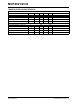
MCP4021/2/3/4 PRODUCT IDENTIFICATION SYSTEM To order or obtain information, e.g., on pricing or delivery, refer to the factory or the listed sales office. PART NO.
MCP4021/2/3/4 NOTES: DS21945E-page 62 © 2006 Microchip Technology Inc.
Note the following details of the code protection feature on Microchip devices: • Microchip products meet the specification contained in their particular Microchip Data Sheet. • Microchip believes that its family of products is one of the most secure families of its kind on the market today, when used in the intended manner and under normal conditions. • There are dishonest and possibly illegal methods used to breach the code protection feature.
WORLDWIDE SALES AND SERVICE AMERICAS ASIA/PACIFIC ASIA/PACIFIC EUROPE Corporate Office 2355 West Chandler Blvd. Chandler, AZ 85224-6199 Tel: 480-792-7200 Fax: 480-792-7277 Technical Support: http://support.microchip.com Web Address: www.microchip.