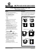
MCP414X/416X/424X/426X 7/8-Bit Single/Dual SPI Digital POT with Non-Volatile Memory Features Description • Single or Dual Resistor Network options • Potentiometer or Rheostat configuration options • Resistor Network Resolution - 7-bit: 128 Resistors (129 Steps) - 8-bit: 256 Resistors (257 Steps) • RAB Resistances options of: - 5 kΩ - 10 kΩ - 50 kΩ - 100 kΩ • Zero-Scale to Full-Scale Wiper operation • Low Wiper Resistance: 75Ω (typical) • Low Tempco: - Absolute (Rheostat): 50 ppm typical (0°C to 70°C) - Ra
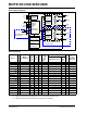
MCP414X/416X/424X/426X Device Block Diagram VDD VSS CS SCK SDI SDO WP SHDN For Dual Potentiometer Devices Only Power-up/ Brown-out Control P0A Resistor Network 0 (Pot 0) P0W Wiper 0 & TCON Register SPI Serial Interface Module & Control Logic (WiperLock™ Technology) P0B P1A Resistor Network 1 (Pot 1) Memory (16x9) Wiper0 (V & NV) Wiper1 (V & NV) TCON STATUS Data EEPROM (10 x 9-bits) P1W Wiper 1 & TCON Register P1B For Dual Resistor Network Devices Only 1 MCP4141 1 Potentiometer (1) SPI Rheos
MCP414X/416X/424X/426X 1.0 ELECTRICAL CHARACTERISTICS Absolute Maximum Ratings † Voltage on VDD with respect to VSS ............... -0.6V to +7.0V Voltage on CS, SCK, SDI, SDI/SDO, WP, and SHDN with respect to VSS ...................................... -0.6V to 12.5V Voltage on all other pins (PxA, PxW, PxB, and SDO) with respect to VSS ............................ -0.3V to VDD + 0.3V Input clamp current, IIK (VI < 0, VI > VDD, VI > VPP ON HV pins) ......................
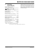
MCP414X/416X/424X/426X AC/DC CHARACTERISTICS Standard Operating Conditions (unless otherwise specified) Operating Temperature –40°C ≤ TA ≤ +125°C (extended) DC Characteristics All parameters apply across the specified operating ranges unless noted. VDD = +2.7V to 5.5V, 5 kΩ, 10 kΩ, 50 kΩ, 100 kΩ devices. Typical specifications represent values for VDD = 5.5V, TA = +25°C. Parameters Sym Min Typ Max Units Conditions Supply Voltage VDD 2.7 — 5.5 V 1.8 — 2.7 V Serial Interface only.
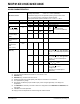
MCP414X/416X/424X/426X AC/DC CHARACTERISTICS (CONTINUED) Standard Operating Conditions (unless otherwise specified) Operating Temperature –40°C ≤ TA ≤ +125°C (extended) DC Characteristics Parameters Resistance (± 20%) Resolution Step Resistance Nominal Resistance Match Wiper Resistance (Note 3, Note 4) All parameters apply across the specified operating ranges unless noted. VDD = +2.7V to 5.5V, 5 kΩ, 10 kΩ, 50 kΩ, 100 kΩ devices. Typical specifications represent values for VDD = 5.5V, TA = +25°C.
MCP414X/416X/424X/426X AC/DC CHARACTERISTICS (CONTINUED) Standard Operating Conditions (unless otherwise specified) Operating Temperature –40°C ≤ TA ≤ +125°C (extended) DC Characteristics Parameters Full-Scale Error (MCP4XX1 only) (8-bit code = 100h, 7-bit code = 80h) Zero-Scale Error (MCP4XX1 only) (8-bit code = 00h, 7-bit code = 00h) All parameters apply across the specified operating ranges unless noted. VDD = +2.7V to 5.5V, 5 kΩ, 10 kΩ, 50 kΩ, 100 kΩ devices.
MCP414X/416X/424X/426X AC/DC CHARACTERISTICS (CONTINUED) Standard Operating Conditions (unless otherwise specified) Operating Temperature –40°C ≤ TA ≤ +125°C (extended) DC Characteristics Parameters Rheostat Integral Non-linearity MCP41X1 (Note 4, Note 8) MCP4XX2 devices only (Note 4) All parameters apply across the specified operating ranges unless noted. VDD = +2.7V to 5.5V, 5 kΩ, 10 kΩ, 50 kΩ, 100 kΩ devices. Typical specifications represent values for VDD = 5.5V, TA = +25°C.
MCP414X/416X/424X/426X AC/DC CHARACTERISTICS (CONTINUED) Standard Operating Conditions (unless otherwise specified) Operating Temperature –40°C ≤ TA ≤ +125°C (extended) DC Characteristics Parameters Rheostat Differential Non-linearity MCP41X1 (Note 4, Note 8) MCP4XX2 devices only (Note 4) All parameters apply across the specified operating ranges unless noted. VDD = +2.7V to 5.5V, 5 kΩ, 10 kΩ, 50 kΩ, 100 kΩ devices. Typical specifications represent values for VDD = 5.5V, TA = +25°C.
MCP414X/416X/424X/426X AC/DC CHARACTERISTICS (CONTINUED) Standard Operating Conditions (unless otherwise specified) Operating Temperature –40°C ≤ TA ≤ +125°C (extended) DC Characteristics Parameters All parameters apply across the specified operating ranges unless noted. VDD = +2.7V to 5.5V, 5 kΩ, 10 kΩ, 50 kΩ, 100 kΩ devices. Typical specifications represent values for VDD = 5.5V, TA = +25°C.
MCP414X/416X/424X/426X AC/DC CHARACTERISTICS (CONTINUED) Standard Operating Conditions (unless otherwise specified) Operating Temperature –40°C ≤ TA ≤ +125°C (extended) DC Characteristics Parameters All parameters apply across the specified operating ranges unless noted. VDD = +2.7V to 5.5V, 5 kΩ, 10 kΩ, 50 kΩ, 100 kΩ devices. Typical specifications represent values for VDD = 5.5V, TA = +25°C.
MCP414X/416X/424X/426X 1.1 SPI Mode Timing Waveforms and Requirements VIHH VIH CS VIH VIL 84 70 72 SCK 83 71 78 79 80 MSb SDO LSb BIT6 - - - - - -1 77 75, 76 SDI MSb IN BIT6 - - - -1 LSb IN 74 73 FIGURE 1-1: TABLE 1-1: # SPI Timing Waveform (Mode = 11).
MCP414X/416X/424X/426X VIH VIHH VIH 82 CS VIL SCK 84 70 83 71 MSb SDO BIT6 - - - - - -1 LSb 75, 76 73 SDI 80 72 MSb IN 77 BIT6 - - - -1 LSb IN 74 FIGURE 1-2: TABLE 1-2: # SPI Timing Waveform (Mode = 00).
MCP414X/416X/424X/426X TABLE 1-3: SPI REQUIREMENTS FOR SDI/SDO MULTIPLEXED (READ OPERATION ONLY) (2) Characteristic Symbol Min Max Units Conditions — 250 kHz VDD= 2.7V to 5.5V SCK Input Frequency FSCK TcsA2scH 60 — ns CS Active (VIL or VIHH) to SCK↑ input SCK input high time TscH 1.8 — us SCK input low time TscL 1.8 — ns 40 — ns Setup time of SDI input to SCK↑ edge TDIV2scH 40 — ns Hold time of SDI input from SCK↑ edge TscH2DIL CS Inactive (VIH) to SDO output hi-impedance TcsH2DOZ — 50 ns Note 1 — 1.
MCP414X/416X/424X/426X TEMPERATURE CHARACTERISTICS Electrical Specifications: Unless otherwise indicated, VDD = +2.7V to +5.5V, VSS = GND. Parameters Sym Min Typ Max Units Specified Temperature Range TA -40 — +125 °C Operating Temperature Range TA -40 — +125 °C Storage Temperature Range TA -65 — +150 °C Thermal Resistance, 8L-MSOP θJA — 211 — °C/W Thermal Resistance, 8L-PDIP θJA — 89.3 — °C/W Thermal Resistance, 8L-SOIC θJA — 149.
MCP414X/416X/424X/426X 2.0 TYPICAL PERFORMANCE CURVES The graphs and tables provided following this note are a statistical summary based on a limited number of samples and are provided for informational purposes only. The performance characteristics listed herein are not tested or guaranteed. In some graphs or tables, the data presented may be outside the specified operating range (e.g., outside specified power supply range) and therefore outside the warranted range. Note: 200 ICS 150 100 50 RCS 0 2.
MCP414X/416X/424X/426X Note: Unless otherwise indicated, TA = +25°C, VDD = 5V, VSS = 0V. 0.2 0.1 80 0 60 -0.1 125°C 20 0 -40°C 25°C 85°C -0.2 RW -40C Rw -40C INL -40C DNL 260 25C Rw 25C INL 25C DNL 85C Rw 85C INL 85C DNL 125C Rw 125C INL 125C DNL 0.1 180 0 140 RW 60 -40°C 20 0 32 25°C -0.1 -0.2 85°C 85°C 25°C 32 -40°C -1.
MCP414X/416X/424X/426X Note: Unless otherwise indicated, TA = +25°C, VDD = 5V, VSS = 0V. FIGURE 2-12: 5 kΩ – Low-Voltage Decrement Wiper Settling Time (VDD = 2.7V) (1 µs/Div). FIGURE 2-15: 5 kΩ – Low-Voltage Increment Wiper Settling Time (VDD = 2.7V) (1 µs/Div). FIGURE 2-13: 5 kΩ – Low-Voltage Decrement Wiper Settling Time (VDD = 5.5V) (1 µs/Div). FIGURE 2-16: 5 kΩ – Low-Voltage Increment Wiper Settling Time (VDD = 5.5V) (1 µs/Div). FIGURE 2-14: 5 kΩ – Power-Up Wiper Response Time (20 ms/Div).
MCP414X/416X/424X/426X Note: Unless otherwise indicated, TA = +25°C, VDD = 5V, VSS = 0V. 125C Rw 125C INL 125C DNL INL DNL 0.2 0.1 80 0 60 -0.1 25°C -40°C 125°C 85°C -0.2 RW 20 -0.3 0 260 220 25C Rw 25C INL 25C DNL 85C Rw 85C INL 85C DNL 125C Rw 125C INL 125C DNL INL DNL 0.1 180 0 140 100 25°C 125°C 85°C 20 0 32 -0.
MCP414X/416X/424X/426X Note: Unless otherwise indicated, TA = +25°C, VDD = 5V, VSS = 0V. FIGURE 2-23: 10 kΩ – Low-Voltage Decrement Wiper Settling Time (VDD = 2.7V) (1 µs/Div). FIGURE 2-25: 10 kΩ – Low-Voltage Increment Wiper Settling Time (VDD = 2.7V) (1 µs/Div). FIGURE 2-24: 10 kΩ – Low-Voltage Decrement Wiper Settling Time (VDD = 5.5V) (1 µs/Div). FIGURE 2-26: 10 kΩ – Low-Voltage Increment Wiper Settling Time (VDD = 5.5V) (1 µs/Div). © 2008 Microchip Technology Inc.
MCP414X/416X/424X/426X Note: Unless otherwise indicated, TA = +25°C, VDD = 5V, VSS = 0V. INL DNL 0.2 0.1 80 0 60 -0.1 40 125°C 25°C 85°C 20 0 -40°C 120 0.3 100 -0.2 RW -0.3 64 96 128 160 192 224 256 Wiper Setting (decimal) 32 260 220 25C Rw 25C INL 25C DNL 85C Rw 85C INL 85C DNL 125C Rw 125C INL 125C DNL INL DNL 180 0 140 RW 100 -40°C 60 0 32 -40C Rw -40C INL -40C DNL 125C Rw 125C INL 125C DNL 49400 0.75 0.25 -0.25 -0.5 -40°C 60 85°C 25°C 0 32 64 -0.
MCP414X/416X/424X/426X Note: Unless otherwise indicated, TA = +25°C, VDD = 5V, VSS = 0V. FIGURE 2-33: 50 kΩ – Low-Voltage Decrement Wiper Settling Time (VDD = 2.7V) (1 µs/Div). FIGURE 2-35: 50 kΩ – Low-Voltage Increment Wiper Settling Time (VDD = 2.7V) (1 µs/Div). FIGURE 2-34: 50 kΩ – Low-Voltage Decrement Wiper Settling Time (VDD = 5.5V) (1 µs/Div). FIGURE 2-36: 50 kΩ – Low-Voltage Increment Wiper Settling Time (VDD = 5.5V) (1 µs/Div). © 2008 Microchip Technology Inc.
MCP414X/416X/424X/426X Note: Unless otherwise indicated, TA = +25°C, VDD = 5V, VSS = 0V. 125C Rw 125C INL 125C DNL 0.2 120 100 0.1 INL DNL 80 0 60 -0.1 40 25°C -40°C -40C Rw -40C INL -40C DNL RW -0.2 64 96 128 160 192 224 256 Wiper Setting (decimal) 32 -40C Rw -40C INL -40C DNL 260 25C Rw 25C INL 25C DNL 85C Rw 85C INL 85C DNL 125C Rw 125C INL 125C DNL INL -0.1 40 -40°C 220 DNL 260 0 140 -0.05 100 RW 60 -40°C -0.15 125°C 85°C 25°C 20 0 32 -0.1 -0.
MCP414X/416X/424X/426X Note: Unless otherwise indicated, TA = +25°C, VDD = 5V, VSS = 0V. FIGURE 2-43: 100 kΩ – Low-Voltage Decrement Wiper Settling Time (VDD = 2.7V) (1 µs/Div). FIGURE 2-45: 100 kΩ – Power-Up Wiper Response Time (1 µs/Div). FIGURE 2-44: 100 kΩ – Low-Voltage Decrement Wiper Settling Time (VDD = 5.5V) (1 µs/Div). FIGURE 2-46: 100 kΩ – Low-Voltage Increment Wiper Settling Time (VDD = 2.7V) (1 µs/Div). © 2008 Microchip Technology Inc.
MCP414X/416X/424X/426X 0.12 0.1 0.09 0.08 0.07 0.06 0.05 0.04 0.03 0.02 0.01 0 0.1 0.08 5.5V % % Note: Unless otherwise indicated, TA = +25°C, VDD = 5V, VSS = 0V. 0.06 0.04 3.0V 0.02 3.0V 0 -40 0 40 80 Temperature (°C) 120 FIGURE 2-47: Resistor Network 0 to Resistor Network 1 RAB (5 kΩ) Mismatch vs. VDD and Temperature. -40 0.04 0.05 0.03 0.04 40 80 Temperature (°C) 0.03 5.5V 0.01 0 120 FIGURE 2-49: Resistor Network 0 to Resistor Network 1 RAB (50 kΩ) Mismatch vs.
MCP414X/416X/424X/426X Note: Unless otherwise indicated, TA = +25°C, VDD = 5V, VSS = 0V. 2.4 0 2.2 -5 IOH (mA) VIH (V) -10 5.5V 2 1.8 1.6 1.4 2.7V 2.7V -15 -20 5.5V -25 -30 -35 1.2 -40 1 -45 -40 0 40 80 120 -40 0 Temperature (°C) FIGURE 2-51: VIH (SDI, SCK, CS, WP, and SHDN) vs. VDD and Temperature. 1.3 5.5V IOL (mA) VIL (V) 1.1 1 0.9 0.8 2.7V 0.7 0.6 -40 0 40 80 120 50 45 40 35 30 25 20 15 10 5 0 120 5.5V 2.
MCP414X/416X/424X/426X Note: Unless otherwise indicated, TA = +25°C, VDD = 5V, VSS = 0V. 2.1 Test Circuits 4.2 +5V tWC (ms) 4.0 VIN 3.8 3.6 Offset GND 3.4 3.2 A W B + VOUT - 2.5V DC 3.0 -40 0 40 80 120 Temperature (°C) FIGURE 2-55: Nominal EEPROM Write Cycle Time vs. VDD and Temperature. FIGURE 2-58: Test. -3 db Gain vs. Frequency 1.2 1 5.5V VDD (V) 0.8 0.6 2.7V 0.4 0.2 0 -40 0 40 80 120 Temperature (°C) FIGURE 2-56: and Temperature. POR/BOR Trip point vs. VDD 15.
MCP414X/416X/424X/426X 3.0 PIN DESCRIPTIONS The descriptions of the pins are listed in Table 3-1. Additional descriptions of the device pins follows.
MCP414X/416X/424X/426X 3.1 Chip Select (CS) The CS pin is the serial interface’s chip select input. Forcing the CS pin to VIL enables the serial commands. Forcing the CS pin to VIHH enables the high-voltage serial commands. 3.2 Serial Data In (SDI) The SDI pin is the serial interfaces Serial Data In pin. This pin is connected to the Host Controllers SDO pin. 3.3 Serial Data In / Serial Data Out (SDI/SDO) On the MCP41X1 devices, pin-out limitations do not allow for individual SDI and SDO pins.
MCP414X/416X/424X/426X 4.0 FUNCTIONAL OVERVIEW This Data Sheet covers a family of thirty-two Digital Potentiometer and Rheostat devices that will be referred to as MCP4XXX. The MCP4XX1 devices are the Potentiometer configuration, while the MCP4XX2 devices are the Rheostat configuration. As the Device Block Diagram shows, there are four main functional blocks.
MCP414X/416X/424X/426X 4.2.1 NON-VOLATILE MEMORY (EEPROM) 4.2.1.4 This memory can be grouped into two uses of non-volatile memory. These are: • General Purpose Registers • Non-Volatile Wiper Registers The non-volatile wipers starts functioning below the devices VPOR/VBOR trip point. 4.2.1.1 General Purpose Registers These locations allow the user to store up to 10 (9-bit) locations worth of information. 4.2.1.
MCP414X/416X/424X/426X 4.2.2.1 Status (STATUS) Register STATUS register can be accessed via the READ commands. Register 4-1 describes each STATUS register bit. This register contains 5 status bits. These bits show the state of the WiperLock bits, the Shutdown bit the Write Protect bit, and if an EEPROM write cycle is active. The REGISTER 4-1: R-1 The STATUS register is placed at Address 05h.
MCP414X/416X/424X/426X REGISTER 4-1: bit 0 Note 1: STATUS REGISTER (CONTINUED) WP: EEPROM Write Protect Status bit (Refer to Section “EEPROM Write Protect” for further information) This bit indicates the status of the write protection on the EEPROM memory. When Write Protect is enabled, writes to all non-volatile memory are prevented. This includes the General Purpose EEPROM memory, and the non-volatile Wiper registers.
MCP414X/416X/424X/426X 4.2.2.2 Terminal Control (TCON) Register This register contains 8 control bits. Four bits are for Wiper 0, and four bits are for Wiper 1. Register 4-2 describes each bit of the TCON register. The state of each resistor network terminal connection is individually controlled. That is, each terminal connection (A, B and W) can be individually connected/ disconnected from the resistor network. This allows the system to minimize the currents through the digital potentiometer.
MCP414X/416X/424X/426X REGISTER 4-2: TCON BITS (1, 2) R-1 R/W-1 R/W-1 R/W-1 R/W-1 R/W-1 R/W-1 R/W-1 R/W-1 D8 R1HW R1A R1W R1B R0HW R0A R0W R0B bit 8 bit 0 Legend: R = Readable bit W = Writable bit U = Unimplemented bit, read as ‘0’ -n = Value at POR ‘1’ = Bit is set ‘0’ = Bit is cleared x = Bit is unknown bit 8 D8: Reserved.
MCP414X/416X/424X/426X 5.0 RESISTOR NETWORK 5.1 The Resistor Network has either 7-bit or 8-bit resolution. Each Resistor Network allows zero scale to full scale connections. Figure 5-1 shows a block diagram for the resistive network of a device. The Resistor Network is made up of several parts. These include: • Resistor Ladder • Wiper • Shutdown (Terminal Connections) Devices have either one or two resistor networks, These are referred to as Pot 0 and Pot 1.
MCP414X/416X/424X/426X 5.2 Wiper 5.3 Each tap point (between the RS resistors) is a connection point for an analog switch. The opposite side of the analog switch is connected to a common signal which is connected to the Terminal W (Wiper) pin. A value in the volatile wiper register selects which analog switch to close, connecting the W terminal to the selected node of the resistor ladder. The wiper can connect directly to Terminal B or to Terminal A.
MCP414X/416X/424X/426X 5.4 5.4.2 Shutdown Shutdown is used to minimize the device’s current consumption. The MCP4XXX has two methods to achieve this. These are: • Hardware Shutdown Pin (SHDN) • Terminal Control Register (TCON) The Hardware Shutdown pin is backwards compatible with the MCP42XXX devices. 5.4.1 HARDWARE SHUTDOWN PIN (SHDN) The SHDN pin is available on the dual potentiometer devices.
MCP414X/416X/424X/426X NOTES: DS22059B-page 38 © 2008 Microchip Technology Inc.
MCP414X/416X/424X/426X 6.0 SERIAL INTERFACE (SPI) The MCP4XXX devices support the SPI serial protocol. This SPI operates in the slave mode (does not generate the serial clock). The SPI interface uses up to four pins. These are: • • • • CS - Chip Select SCK - Serial Clock SDI - Serial Data In SDO - Serial Data Out Typical SPI Interfaces are shown in Figure 6-1.
MCP414X/416X/424X/426X 6.1 SDI, SDO, SCK, and CS Operation The operation of the four SPI interface pins are discussed in this section. These pins are: • • • • SDI (Serial Data In) SDO (Serial Data Out) SCK (Serial Clock) CS (Chip Select) 6.1.3 Note: SDI/SDO MCP41X1 Devices Only . For device packages that do not have enough pins for both an SDI and SDO pin, the SDI and SDO functionality is multiplexed onto a single I/O pin called SDI/SDO.
MCP414X/416X/424X/426X 6.1.4 SERIAL CLOCK (SCK) (SPI FREQUENCY OF OPERATION) 6.1.5 THE CS SIGNAL The SPI interface is specified to operate up to 10 MHz. The actual clock rate depends on the configuration of the system and the serial command used. Table 6-1 shows the SCK frequency for different configurations. The Chip Select (CS) signal is used to select the device and frame a command sequence.
MCP414X/416X/424X/426X 6.2 The SPI Modes 6.3 The SPI module supports two (of the four) standard SPI modes. These are Mode 0,0 and 1,1. The mode is determined by the state of the SDI pin on the rising edge of the 1st clock bit (of the 8-bit byte). 6.2.1 Figure 6-3 through Figure 6-8 show the different SPI command waveforms. Figure 6-3 and Figure 6-4 are read and write commands. Figure 6-5 and Figure 6-6 are read commands when the SDI and SDO pins are multiplexed on the same pin (SDI/SDO).
MCP414X/416X/424X/426X VIH CS VIHH VIL SCK Write to SSPBUF CMDERR bit D9 D8 D7 bit9 bit8 bit7 SDO AD3 AD2 AD1 AD0 bit15 bit14 bit13 bit12 SDI C1 1 C0 1 (1) (1) (1) D6 bit6 D5 bit5 D4 bit4 D3 bit3 D2 bit2 D1 bit1 D0 bit0 (1) (1) (1) (1) (1) (1) (1) Input Sample Note 1: The SDI pin will read the state of the SDI pin which will be the SDO signal, unless overdriven FIGURE 6-5: 16-Bit Read Command for Devices with SDI/SDO multiplexed SPI Waveform (Mode 1,1).
MCP414X/416X/424X/426X CS VIH VIHH VIL SCK Write to SSPBUF CMDERR bit “1” = “Valid” Command/Address “0” = “Invalid” Command/Address SDO bit7 SDI AD3 bit6 AD2 bit5 AD1 bit4 AD0 bit3 C1 bit2 C0 bit1 X bit0 X bit0 bit7 Input Sample FIGURE 6-7: 8-Bit Commands (Increment, Decrement, Modify Write Protect or WiperLock Technology) - SPI Waveform with PIC MCU (Mode 1,1).
MCP414X/416X/424X/426X 7.0 DEVICE COMMANDS 7.1 Command Byte The Command Byte has three fields, the Address, the Command, and 2 Data bits, see Figure 7-1. Currently only one of the data bits is defined (D8). This is for the Write command. The MCP4XXX’s SPI command format supports 16 memory address locations and four commands. Each command has two modes.
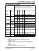
MCP414X/416X/424X/426X TABLE 7-2: MEMORY MAP AND THE SUPPORTED COMMANDS Address Command Value 00h 01h 02h 03h Function Volatile Wiper 0 Volatile Wiper 1 NV Wiper 0 NV Wiper 1 Data (10-bits) (1) SPI String (Binary) MISO (SDO pin) (2) MOSI (SDI pin) Write Data nn nnnn nnnn 0000 00nn nnnn nnnn 1111 1111 1111 1111 Read Data nn nnnn nnnn 0000 11nn nnnn nnnn 1111 111n nnnn nnnn Increment Wiper — 0000 0100 1111 1111 Decrement Wiper — 0000 1000 1111 1111 Write Data nn nnnn nnnn 0001 0
MCP414X/416X/424X/426X 7.2 Data Byte Only the Read Command and the Write Command use the Data Byte, see Figure 7-1. These commands concatenate the 8-bits of the Data Byte with the one data bit (D8) contained in the Command Byte to form 9-bits of data (D8:D0). The Command Byte format supports up to 9-bits of data so that the 8-bit resistor network can be set to Full Scale (100h or greater). This allows wiper connections to Terminal A and to Terminal B.
MCP414X/416X/424X/426X 7.4 Continuous Commands The device supports the ability to execute commands continuously. While the CS pin is in the active state (VIL or VIHH). Any sequence of valid commands may be received. The following example is a valid sequence of events: 1. 2. 3. 4. 5. 6. 7. 8. Note 1: It is recommended that while the CS pin is active, only one type of command should be issued. When changing commands, it is recommended to take the CS pin inactive then force it back to the active state.
MCP414X/416X/424X/426X 7.5 7.5.2 Write Data Normal and High Voltage The sequence to write to to a single non-volatile memory location is the same as a single write to volatile memory with the exception that after the CS pin is driven inactive (VIH), the EEPROM write cycle (tWC) is started. A write cycle will not start if the write command isn’t exactly 16 clocks pulses. This protects against system issues from corrupting the Non-Volatile memory locations. The Write command is a 16-bit command.
MCP414X/416X/424X/426X 7.5.3 CONTINUOUS WRITES TO VOLATILE MEMORY 7.5.4 Continuous writes are possible only when writing to the volatile memory registers (address 00h, 01h, and 04h). Continuous writes to non-volatile memory are not allowed, and attempts to do so will result in a command error (CMDERR) condition. Figure 7-3 shows the sequence for three continuous writes. The writes do not need to be to the same volatile memory address.
MCP414X/416X/424X/426X 7.6 7.6.1 Read Data Normal and High Voltage The read operation requires that the CS pin be in the active state (VILor VIHH). Typically, the CS pin will be in the inactive state (VIH) and is driven to the active state (VILor VIHH). The 16-bit Read Command (Command Byte and Data Byte) is then clocked in on the SCK and SDI pins. The SDO pin starts driving data on the 7th bit (CMDERR bit) and the addressed data comes out on the 8th through 16th clocks.
MCP414X/416X/424X/426X 7.6.2 CONTINUOUS READS Figure 7-5 shows the sequence for three continuous reads. The reads do not need to be to the same memory address. Continuous reads allows the devices memory to be read quickly. Continuous reads are possible to all memory locations. If a non-volatile memory write cycle is occurring, then Read commands may only access the volatile memory locations.
MCP414X/416X/424X/426X 7.7 Increment Wiper Normal and High Voltage The Increment Command is an 8-bit command. The Increment Command can only be issued to volatile memory locations. The format of the command is shown in Figure 7-6. An Increment Command to the volatile memory location changes that location after a properly formatted command (8-clocks) have been received. Increment commands provide a quick and easy method to modify the value of the volatile wiper location by +1 with minimal overhead.
MCP414X/416X/424X/426X 7.7.2 CONTINUOUS INCREMENTS Increment commands can be sent repeatedly without raising CS until a desired condition is met. The value in the Volatile Wiper register can be read using a Read Command and written to the corresponding Non-Volatile Wiper EEPROM using a Write Command. Continuous Increments are possible only when writing to the volatile memory registers (address 00h, and 01h). Figure 7-7 shows a Continuous Increment sequence for three continuous writes.
MCP414X/416X/424X/426X 7.8 Decrement Wiper Normal and High Voltage The Decrement Command is an 8-bit command. The Decrement Command can only be issued to volatile memory locations. The format of the command is shown in Figure 7-6. An Decrement Command to the volatile memory location changes that location after a properly formatted command (8-clocks) have been received. Decrement commands provide a quick and easy method to modify the value of the volatile wiper location by -1 with minimal overhead.
MCP414X/416X/424X/426X 7.8.2 CONTINUOUS DECREMENTS Decrement commands can be sent repeatedly without raising CS until a desired condition is met. The value in the Volatile Wiper register can be read using a Read Command and written to the corresponding Non-Volatile Wiper EEPROM using a Write Command. Continuous Decrements are possible only when writing to the volatile memory registers (address 00h, 01h, and 04h). Figure 7-9 shows a continuous Decrement sequence for three continuous writes.
MCP414X/416X/424X/426X 7.9 Modify Write Protect or WiperLock Technology (High Voltage) Enable and Disable This command is a special case of the High Voltage Decrement Wiper and High Voltage Increment Wiper commands to the non-volatile memory locations 02h, 03h, and 0Fh. This command is used to enable or disable either the software Write Protect, wiper 0 WiperLock Technology, or wiper 1 WiperLock Technology.
MCP414X/416X/424X/426X NOTES: DS22059B-page 58 © 2008 Microchip Technology Inc.
MCP414X/416X/424X/426X 8.0 APPLICATIONS EXAMPLES Non-volatile digital potentiometers have a multitude of practical uses in modern electronic circuits. The most popular uses include precision calibration of set point thresholds, sensor trimming, LCD bias trimming, audio attenuation, adjustable power supplies, motor control overcurrent trip setting, adjustable gain amplifiers and offset trimming.
MCP414X/416X/424X/426X 8.2 Techniques to force the CS pin to VIHH PIC10F206 The circuit in Figure 8-3 shows a method using the TC1240A doubling charge pump. When the SHDN pin is high, the TC1240A is off, and the level on the CS pin is controlled by the PIC® microcontrollers (MCUs) IO2 pin. When the SHDN pin is low, the TC1240A is on and the VOUT voltage is 2 * VDD. The resistor R1 allows the CS pin to go higher than the voltage such that the PIC MCU’s IO2 pin “clamps” at approximately VDD.
MCP414X/416X/424X/426X 8.4 8.4.2 Design Considerations In the design of a system with the MCP4XXX devices, the following considerations should be taken into account: • Power Supply Considerations • Layout Considerations 8.4.1 POWER SUPPLY CONSIDERATIONS The typical application will require a bypass capacitor in order to filter high-frequency noise, which can be induced onto the power supply's traces. The bypass capacitor helps to minimize the effect of these noise sources on signal integrity.
MCP414X/416X/424X/426X NOTES: DS22059B-page 62 © 2008 Microchip Technology Inc.
MCP414X/416X/424X/426X 9.0 DEVELOPMENT SUPPORT 9.1 Development Tools 9.2 Technical Documentation Several additional technical documents are available to assist you in your design and development. These technical documents include Application Notes, Technical Briefs, and Design Guides. Table 9-2 shows some of these documents. Several development tools are available to assist in your design and evaluation of the MCP4XXX devices. The currently available tools are shown in Table 9-1.
MCP414X/416X/424X/426X NOTES: DS22059B-page 64 © 2008 Microchip Technology Inc.
MCP414X/416X/424X/426X 10.0 PACKAGING INFORMATION 10.
MCP414X/416X/424X/426X 8-Lead PDIP XXXXXXXX XXXXXNNN YYWW 8-Lead SOIC 4141-502 E/P e3 256 0816 Example XXXXXXXX XXXXYYWW 4141502E SN^^^0816 e3 NNN 256 Legend: XX...X Y YY WW NNN e3 * Note: DS22059B-page 66 Example Customer-specific information Year code (last digit of calendar year) Year code (last 2 digits of calendar year) Week code (week of January 1 is week ‘01’) Alphanumeric traceability code Pb-free JEDEC designator for Matte Tin (Sn) This package is Pb-free.
MCP414X/416X/424X/426X Package Marking Information (Continued) Example: 10-Lead DFN (3x3) XXXX YYWW NNN Part Number Code Part Number Code MCP4242-502E/MF BAEM MCP4262-502E/MF BAEW MCP4242-103E/MF BAEP MCP4262-103E/MF BAEX MCP4242-104E/MF BAER MCP4262-104E/MF BAEZ MCP4242-503E/MF BAEQ MCP4262-503E/MF BAEY 10-Lead MSOP BAEH 0816 256 Example XXXXXX Part Number Code Part Number Code YWWNNN MCP4242-502E/MS 424252 MCP4262-502E/MS 426252 MCP4242-103E/MS 424213 MCP4262-103E/MS
MCP414X/416X/424X/426X % 2 % & % ! % * %% 133))) & &3 " ) * ' ! " # $ % * D e b N $ % % " % N L EXPOSED PAD E2 E K NOTE 1 1 2 D2 2 NOTE 1 1 BOTTOM VIEW TOP VIEW A NOTE 2 A3 A1 4 % & 5 & % 6!&( $ 55 , , 6 6 67 8 9 % :. / 0 7 ; % 9 % " $$ .
MCP414X/416X/424X/426X % 2 % & % ! % * %% 133))) & &3 © 2008 Microchip Technology Inc.
MCP414X/416X/424X/426X % & ' ( ) ' # '( $ 2 % & % ! % * %% 133))) & &3 " ) * ' % * $ % % " % D N E E1 NOTE 1 1 2 e b A2 A c φ L L1 A1 4 % & 5 & % 6!&( $ 55 , , 6 6 :. / 0 7 ; % * % " $$ 7 < "% " " * 7 5 % 8 9 % " " * 67 = = . 9. . = .
MCP414X/416X/424X/426X % *) ) 2 % & % ! % * %% 133))) & &3 " ) * ! " # * $ ' % * $ % % " % N NOTE 1 E1 1 3 2 D E A2 A L A1 c e eB b1 b 4 % & 5 & % 6!&( $ 60;, 6 6 67 8 9 % / 0 % % = = . + . . = = ! " % ! " < "% , + + .
MCP414X/416X/424X/426X % ' ( ) ' && + 2 % & % ! % * %% 133))) & &3 " ) * ' ! " #'(*,$ % * $ % % " % D e N E E1 NOTE 1 1 2 3 α h b h A2 A c φ L A1 L1 4 % & 5 & % 6!&( $ 55 , , 6 6 8 / 0 7 ; % * % " $$ @ 7 < "% " " * 67 9 % " " * β = = . = = = .
MCP414X/416X/424X/426X % ' ( ) ' && + 2 % & % ! % * %% 133))) & &3 © 2008 Microchip Technology Inc.
MCP414X/416X/424X/426X - % 2 % & % ! % * %% 133))) & &3 " ) * ' ! " # $ % * D $ % % " % e b N N L K E E2 EXPOSED PAD NOTE 1 1 2 2 1 NOTE 1 D2 BOTTOM VIEW TOP VIEW A A1 A3 NOTE 2 4 % & 5 & % 6!&( $ 55 , , 6 6 67 8 % . / 0 7 ; % 9 % " $$ .
MCP414X/416X/424X/426X - % 2 % & % ! % * %% 133))) & &3 © 2008 Microchip Technology Inc.
MCP414X/416X/424X/426X - % & ' ( ) . # '( $ 2 % & % ! % * %% 133))) & &3 " ) * ' % * $ % % " % D N E E1 NOTE 1 1 2 b e A A2 c φ L A1 L1 4 % & 5 & % 6!&( $ 55 , , 6 6 . / 0 7 ; % * % " $$ 7 < "% " " * 7 5 % 8 % " " * 67 = = . 9. . = .
MCP414X/416X/424X/426X -/ % *) ) 2 % & % ! % * %% 133))) & &3 " ) * ! " # * $ ' % * $ % % " % N NOTE 1 E1 1 3 2 D E A2 A L A1 c b1 b e eB 4 % & 5 & % 6!&( $ 60;, 6 6 67 8 % / 0 % % = = . + . . = = ! " % ! " < "% , + + .
MCP414X/416X/424X/426X -/ % ' ( ) ' && + 2 % & % ! % * %% 133))) & &3 " ) * ' ! " #'(*,$ % * $ % % " % D N E E1 NOTE 1 1 2 3 e h b A2 A c φ L A1 β L1 4 % & 5 & % 6!&( $ 55 , , 6 6 8 / 0 7 ; % * % " $$ @ 7 < "% " " * 67 % " " * α h = = . = = = .
MCP414X/416X/424X/426X % 2 % & % ! % * %% 133))) & &3 © 2008 Microchip Technology Inc.
MCP414X/416X/424X/426X -/ % 01 ) '1& ) ' ( ) '0 / / 2 % & % ! % * %% 133))) & &3 " ) * ' ! " #0''( $ % * $ % % " % D N E E1 NOTE 1 1 2 e b A2 A c A1 φ L L1 4 % & 5 & % 6!&( $ 55 , , 6 6 8 % :. / 0 7 ; % " " * 67 * % " $$ 7 < "% = = 9 . . = .
MCP414X/416X/424X/426X -2 % 3 / / 2 % & % ! % * %% 133))) & &3 " ) * ' ! " #3 $ % * $ % % " % D2 D EXPOSED PAD e E E2 2 2 1 b 1 TOP VIEW K N N NOTE 1 L BOTTOM VIEW A3 A A1 4 % & 5 & % 6!&( $ 55 , , 6 6 67 8 : % :. / 0 7 ; % 9 % " $$ .
MCP414X/416X/424X/426X % 2 % & % ! % * %% 133))) & &3 DS22059B-page 82 " ) * ' % * $ % % " % © 2008 Microchip Technology Inc.
MCP414X/416X/424X/426X APPENDIX A: REVISION HISTORY APPENDIX B: Revision B (December 2008) The following is the list of modifications: 1. 2. 3. 4. 5. Updated IPU specifications to specify test conditions and new limit. Updated DFN and QFN package in “Package Types (top view)”, to include Exposed Thermal Pad samples (EP). Added new descriptions in Section 3.0 “Pin Descriptions”. Added new Development Tool support item. Updated Package Outline section.
MCP414X/416X/424X/426X NOTES: DS22059B-page 84 © 2008 Microchip Technology Inc.
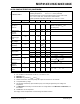
MCP414X/416X/424X/426X PRODUCT IDENTIFICATION SYSTEM To order or obtain information, e.g., on pricing or delivery, refer to the factory or the listed sales office. PART NO.
MCP414X/416X/424X/426X NOTES: DS22059B-page 86 © 2008 Microchip Technology Inc.
Note the following details of the code protection feature on Microchip devices: • Microchip products meet the specification contained in their particular Microchip Data Sheet. • Microchip believes that its family of products is one of the most secure families of its kind on the market today, when used in the intended manner and under normal conditions. • There are dishonest and possibly illegal methods used to breach the code protection feature.
WORLDWIDE SALES AND SERVICE AMERICAS ASIA/PACIFIC ASIA/PACIFIC EUROPE Corporate Office 2355 West Chandler Blvd. Chandler, AZ 85224-6199 Tel: 480-792-7200 Fax: 480-792-7277 Technical Support: http://support.microchip.com Web Address: www.microchip.