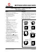
MCP454X/456X/464X/466X 7/8-Bit Single/Dual I2C Digital POT with Nonvolatile Memory Features Description • Single or Dual Resistor Network Options • Potentiometer or Rheostat Configuration Options • Resistor Network Resolution - 7-bit: 128 Resistors (129 Steps) - 8-bit: 256 Resistors (257 Steps) • RAB Resistances Options of: - 5 k - 10 k - 50 k - 100 k • Zero-Scale to Full-Scale Wiper Operation • Low Wiper Resistance: 75 (typical) • Low Tempco: - Absolute (Rheostat): 50 ppm typical (0°C to 70°C) - Rat
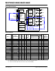
MCP454X/456X/464X/466X Device Block Diagram VDD VSS A2 A1 HVC/A0 SCL SDA 2 I C Interface Power-up/ Brown-out Control Resistor Network 0 (Pot 0) I2C Serial Interface Module & Control Logic (WiperLock™ Technology) Wiper 0 & TCON Register P0A P0W P0B P1A Resistor Network 1 (Pot 1) WP Memory (16x9) Wiper0 (V & NV) Wiper1 (V & NV) TCON STATUS Data EEPROM (10 x 9-bits) P1W Wiper 1 & TCON Register P1B For Dual Resistor Network Devices Only I2C RAM No Mid-Scale 5.0, 10.0, 50.0, 100.0 75 129 1.
MCP454X/456X/464X/466X 1.0 ELECTRICAL CHARACTERISTICS 1.1 Absolute Maximum Ratings† Voltage on VDD with respect to VSS ........................................................................................................... -0.6V to +7.0V Voltage on HVC/A0, A1, A2, SCL, SDA and WP with respect to VSS ....................................................... -0.6V to 12.5V Voltage on all other pins (PxA, PxW, and PxB) with respect to VSS ..................................................-0.
MCP454X/456X/464X/466X AC/DC CHARACTERISTICS Standard Operating Conditions (unless otherwise specified) Operating Temperature –40°C TA +125°C (extended) DC Characteristics Parameters Supply Voltage HVC pin voltage range All parameters apply across the specified operating ranges unless noted. VDD = +2.7V to 5.5V, 5 k, 10 k, 50 k, 100 k devices. Typical specifications represent values for VDD = 5.5V, TA = +25°C. Sym Min Typ Max Units VDD 2.7 — 5.5 V 1.8 — 2.7 V VSS — 12.
MCP454X/456X/464X/466X AC/DC CHARACTERISTICS (CONTINUED) Standard Operating Conditions (unless otherwise specified) Operating Temperature –40°C TA +125°C (extended) DC Characteristics Parameters Resistance (± 20%) Resolution Step Resistance Nominal Resistance Match Wiper Resistance (Note 3, Note 4) All parameters apply across the specified operating ranges unless noted. VDD = +2.7V to 5.5V, 5 k, 10 k, 50 k, 100 k devices. Typical specifications represent values for VDD = 5.5V, TA = +25°C.
MCP454X/456X/464X/466X AC/DC CHARACTERISTICS (CONTINUED) Standard Operating Conditions (unless otherwise specified) Operating Temperature –40°C TA +125°C (extended) DC Characteristics Parameters Maximum current through Terminal (A, W or B) Note 6 Leakage current into A, W or B All parameters apply across the specified operating ranges unless noted. VDD = +2.7V to 5.5V, 5 k, 10 k, 50 k, 100 k devices. Typical specifications represent values for VDD = 5.5V, TA = +25°C.
MCP454X/456X/464X/466X AC/DC CHARACTERISTICS (CONTINUED) Standard Operating Conditions (unless otherwise specified) Operating Temperature –40°C TA +125°C (extended) DC Characteristics All parameters apply across the specified operating ranges unless noted. VDD = +2.7V to 5.5V, 5 k, 10 k, 50 k, 100 k devices. Typical specifications represent values for VDD = 5.5V, TA = +25°C. Parameters Sym Min Typ Max Units Full-Scale Error (MCP4XX1 only) (8-bit code = 100h, 7-bit code = 80h) VWFSE -6.
MCP454X/456X/464X/466X AC/DC CHARACTERISTICS (CONTINUED) Standard Operating Conditions (unless otherwise specified) Operating Temperature –40°C TA +125°C (extended) DC Characteristics Parameters Bandwidth -3 dB (See Figure 2-58, load = 30 pF) All parameters apply across the specified operating ranges unless noted. VDD = +2.7V to 5.5V, 5 k, 10 k, 50 k, 100 k devices. Typical specifications represent values for VDD = 5.5V, TA = +25°C.
MCP454X/456X/464X/466X AC/DC CHARACTERISTICS (CONTINUED) Standard Operating Conditions (unless otherwise specified) Operating Temperature –40°C TA +125°C (extended) DC Characteristics All parameters apply across the specified operating ranges unless noted. VDD = +2.7V to 5.5V, 5 k, 10 k, 50 k, 100 k devices. Typical specifications represent values for VDD = 5.5V, TA = +25°C.
MCP454X/456X/464X/466X AC/DC CHARACTERISTICS (CONTINUED) Standard Operating Conditions (unless otherwise specified) Operating Temperature –40°C TA +125°C (extended) DC Characteristics All parameters apply across the specified operating ranges unless noted. VDD = +2.7V to 5.5V, 5 k, 10 k, 50 k, 100 k devices. Typical specifications represent values for VDD = 5.5V, TA = +25°C.
MCP454X/456X/464X/466X AC/DC CHARACTERISTICS (CONTINUED) Standard Operating Conditions (unless otherwise specified) Operating Temperature –40°C TA +125°C (extended) DC Characteristics Parameters All parameters apply across the specified operating ranges unless noted. VDD = +2.7V to 5.5V, 5 k, 10 k, 50 k, 100 k devices. Typical specifications represent values for VDD = 5.5V, TA = +25°C.
MCP454X/456X/464X/466X AC/DC CHARACTERISTICS (CONTINUED) Standard Operating Conditions (unless otherwise specified) Operating Temperature –40°C TA +125°C (extended) DC Characteristics Parameters All parameters apply across the specified operating ranges unless noted. VDD = +2.7V to 5.5V, 5 k, 10 k, 50 k, 100 k devices. Typical specifications represent values for VDD = 5.5V, TA = +25°C.
MCP454X/456X/464X/466X SCL 93 91 90 92 SDA STOP Condition START Condition I2C Bus Start/Stop Bits Timing Waveforms. FIGURE 1-1: I2C BUS START/STOP BITS REQUIREMENTS TABLE 1-1: I2C AC Characteristics Param. Symbol No.
MCP454X/456X/464X/466X 103 102 100 101 SCL 90 106 91 92 107 SDA In 110 109 109 SDA Out I2C Bus Data Timing. FIGURE 1-2: I2C BUS DATA REQUIREMENTS (SLAVE MODE) TABLE 1-2: I2C AC Characteristics Param. No.
MCP454X/456X/464X/466X TABLE 1-2: I2C BUS DATA REQUIREMENTS (SLAVE MODE) (CONTINUED) I2C AC Characteristics Param. No.
MCP454X/456X/464X/466X I2C BUS DATA REQUIREMENTS (SLAVE MODE) (CONTINUED) TABLE 1-2: I2C AC Characteristics Param. No.
MCP454X/456X/464X/466X TEMPERATURE CHARACTERISTICS Electrical Specifications: Unless otherwise indicated, VDD = +2.7V to +5.5V, VSS = GND. Parameters Sym Min Typ Max Units Specified Temperature Range TA -40 — +125 °C Operating Temperature Range TA -40 — +125 °C Storage Temperature Range TA -65 — +150 °C Thermal Resistance, 8L-DFN (3x3) JA — 56.7 — °C/W Thermal Resistance, 8L-MSOP JA — 211 — °C/W Thermal Resistance, 8L-SOIC JA — 149.
MCP454X/456X/464X/466X NOTES: DS22107B-page 18 2008-2013 Microchip Technology Inc.
MCP454X/456X/464X/466X 2.0 TYPICAL PERFORMANCE CURVES Note: The graphs and tables provided following this note are a statistical summary based on a limited number of samples and are provided for informational purposes only. The performance characteristics listed herein are not tested or guaranteed. In some graphs or tables, the data presented may be outside the specified operating range (e.g., outside specified power supply range) and therefore outside the warranted range. 450 1.7MHz, 5.5V 300 250 1.
MCP454X/456X/464X/466X Note: Unless otherwise indicated, TA = +25°C, VDD = 5V, VSS = 0V. INL DNL 0.3 0.2 0.1 80 0 60 -0.1 40 125°C 20 0 -40°C 25°C 85°C 120 100 -0.2 RW -0.3 64 96 128 160 192 224 256 Wiper Setting (decimal) 32 260 25C Rw 25C INL 25C DNL 85C Rw 85C INL 85C DNL 125C Rw 125C INL 125C DNL INL 220 DNL 180 0 140 RW 100 -0.1 125°C 60 -40°C 20 0 32 25°C 85°C -0.2 -0.
MCP454X/456X/464X/466X 5300 6000 5250 5000 RWB (Ohms) Nominal Resistance (RAB) (Ohms) Note: Unless otherwise indicated, TA = +25°C, VDD = 5V, VSS = 0V. 2.7V 5200 5150 5100 4000 3000 2000 -40°C 25°C 85°C 125°C 1000 5.5V 5050 0 -40 0 40 80 Ambient Temperature (°C) 120 FIGURE 2-10: 5 k – Nominal Resistance () vs. Ambient Temperature and VDD. 2008-2013 Microchip Technology Inc. 0 32 64 96 128 160 192 Wiper Setting (decimal) 224 256 FIGURE 2-11: 5 k – RWB () vs.
MCP454X/456X/464X/466X Note: Unless otherwise indicated, TA = +25°C, VDD = 5V, VSS = 0V. FIGURE 2-12: 5 k – Low-Voltage Decrement Wiper Settling Time (VDD = 5.5V) (1 µs/Div). FIGURE 2-15: 5 k – Low-Voltage Increment Wiper Settling Time (VDD = 5.5V) (1 µs/Div). FIGURE 2-13: 5 k – Low-Voltage Decrement Wiper Settling Time (VDD = 2.7V) (1 µs/Div). FIGURE 2-16: 5 k – Low-Voltage Increment Wiper Settling Time (VDD = 2.7V) (1 µs/Div). FIGURE 2-14: 5 k – Power-Up Wiper Response Time (20 ms/Div).
MCP454X/456X/464X/466X Note: Unless otherwise indicated, TA = +25°C, VDD = 5V, VSS = 0V. 125C Rw 125C INL 125C DNL INL DNL 0.3 0.2 0.1 80 0 60 -0.1 25°C -40°C 125°C 85°C -0.2 RW 20 -0.3 0 260 220 25C Rw 25C INL 25C DNL 85C Rw 85C INL 85C DNL INL DNL 125C Rw 125C INL 125C DNL 0.1 0 140 100 RW 60 25°C 125°C 85°C 20 0 0 60 40 125°C 32 -40°C 300 -0.1 -0.2 -0.3 64 96 128 160 192 224 256 Wiper Setting (decimal) FIGURE 2-18: 10 k Pot Mode – RW (), INL (LSb), DNL (LSb) vs.
MCP454X/456X/464X/466X Note: Unless otherwise indicated, TA = +25°C, VDD = 5V, VSS = 0V. 12000 10250 10000 10200 10150 10100 RWB (Ohms) Nominal Resistance (R AB) (Ohms) 10300 2.7V 10050 10000 5.5V 9950 1.8V 8000 6000 4000 -40°C 25°C 85°C 125°C 2000 9900 9850 0 -40 0 40 80 Ambient Temperature (°C) 120 FIGURE 2-21: 10 k – Nominal Resistance () vs. Ambient Temperature and VDD. DS22107B-page 24 0 32 64 96 128 160 192 Wiper Setting (decimal) 224 256 FIGURE 2-22: 10 k – RWB () vs.
MCP454X/456X/464X/466X Note: Unless otherwise indicated, TA = +25°C, VDD = 5V, VSS = 0V. FIGURE 2-23: 10 k – Low-Voltage Decrement Wiper Settling Time (VDD = 5.5V) (1 µs/Div). FIGURE 2-26: 10 k – Low-Voltage Increment Wiper Settling Time (VDD = 5.5V) (1 µs/Div). FIGURE 2-24: 10 k – Low-Voltage Decrement Wiper Settling Time (VDD = 2.7V) (1 µs/Div). FIGURE 2-27: 10 k – Low-Voltage Increment Wiper Settling Time (VDD = 2.7V) (1 µs/Div). FIGURE 2-25: 10 k – Power-Up Wiper Response Time (1 µs/Div).
MCP454X/456X/464X/466X Note: Unless otherwise indicated, TA = +25°C, VDD = 5V, VSS = 0V. INL DNL 0.3 0.2 0.1 80 0 60 -0.1 40 125°C 25°C 85°C 20 0 -40°C 120 100 -0.2 RW -0.3 64 96 128 160 192 224 256 Wiper Setting (decimal) 32 260 220 25C Rw 25C INL 25C DNL 85C Rw 85C INL 85C DNL INL DNL 125C Rw 125C INL 125C DNL 180 0 140 RW 100 -40°C 60 -0.1 -0.2 -0.1 40 0 32 -0.3 64 96 128 160 192 224 256 Wiper Setting (decimal) FIGURE 2-29: 50 k Pot Mode – RW (), INL (LSb), DNL (LSb) vs.
MCP454X/456X/464X/466X Note: Unless otherwise indicated, TA = +25°C, VDD = 5V, VSS = 0V. 60000 52000 50000 51500 1.8V RWB (Ohms) Nominal Resistance (R (Ohms) AB) 52500 51000 50500 50000 2.7V 40000 30000 20000 -40°C 25°C 85°C 125°C 10000 49500 5.5V 49000 0 -40 0 40 80 Ambient Temperature (°C) 120 FIGURE 2-32: 50 k – Nominal Resistance () vs. Ambient Temperature and VDD. 2008-2013 Microchip Technology Inc.
MCP454X/456X/464X/466X Note: Unless otherwise indicated, TA = +25°C, VDD = 5V, VSS = 0V. FIGURE 2-34: 50 k – Low-Voltage Decrement Wiper Settling Time (VDD = 5.5V) (1 µs/Div). FIGURE 2-37: 50 k – Low-Voltage Increment Wiper Settling Time (VDD = 5.5V) (1 µs/Div). FIGURE 2-35: 50 k – Low-Voltage Decrement Wiper Settling Time (VDD = 2.7V) (1 µs/Div). FIGURE 2-38: 50 k – Low-Voltage Increment Wiper Settling Time (VDD = 2.7V) (1 µs/Div). FIGURE 2-36: 50 k – Power-Up Wiper Response Time (1 µs/Div).
MCP454X/456X/464X/466X Note: Unless otherwise indicated, TA = +25°C, VDD = 5V, VSS = 0V. 125C Rw 125C INL 125C DNL 0.2 DNL 0 60 -0.1 40 25°C -40°C -40C Rw -40C INL -40C DNL 100 0.1 INL 80 120 RW 32 -0.2 64 96 128 160 192 224 256 Wiper Setting (decimal) -40C Rw -40C INL -40C DNL 260 25C Rw 25C INL 25C DNL 85C Rw 85C INL 85C DNL INL 220 DNL 125C Rw 125C INL 125C DNL -0.1 40 -40°C 260 0 140 -0.05 100 RW 60 20 -40°C 125°C 85°C 25°C 0 32 -0.1 -0.15 -0.
MCP454X/456X/464X/466X 120000 103500 103000 102500 102000 101500 101000 100500 100000 99500 99000 98500 100000 Rwb (Ohms) Nominal Resistance (R (Ohms) AB) Note: Unless otherwise indicated, TA = +25°C, VDD = 5V, VSS = 0V. 1.8V 2.7V 80000 60000 40000 -40°C 25°C 85°C 125°C 20000 5.5V 0 -40 0 40 80 Ambient Temperature (°C) 120 FIGURE 2-43: 100 k – Nominal Resistance () vs. Ambient Temperature and VDD .
MCP454X/456X/464X/466X Note: Unless otherwise indicated, TA = +25°C, VDD = 5V, VSS = 0V. FIGURE 2-45: 100 k – Low-Voltage Decrement Wiper Settling Time (VDD = 5.5V) (1 µs/Div). FIGURE 2-47: 100 k – Low-Voltage Increment Wiper Settling Time (VDD =5.5V) (1 µs/Div). FIGURE 2-46: 100 k – Low-Voltage Decrement Wiper Settling Time (VDD = 2.7V) (1 µs/Div). FIGURE 2-48: 100 k – Low-Voltage Increment Wiper Settling Time (VDD = 2.7V) (1 µs/Div) 2008-2013 Microchip Technology Inc.
MCP454X/456X/464X/466X 0.12 0.1 0.09 0.08 0.07 0.06 0.05 0.04 0.03 0.02 0.01 0 0.1 0.08 5.5V % % Note: Unless otherwise indicated, TA = +25°C, VDD = 5V, VSS = 0V. 0.06 0.04 3.0V 0.02 3.0V 0 -40 0 40 80 Temperature (°C) 120 FIGURE 2-49: Resistor Network 0 to Resistor Network 1 RAB (5 k) Mismatch vs. VDD and Temperature. -40 0.04 0.05 0.03 0.04 40 80 Temperature (°C) 0.03 5.5V 0.01 0 120 FIGURE 2-51: Resistor Network 0 to Resistor Network 1 RAB (50 k) Mismatch vs.
MCP454X/456X/464X/466X Note: Unless otherwise indicated, TA = +25°C, VDD = 5V, VSS = 0V. 4 3.5 5.5V VOL (mV) VIH (V) 3 2.5 2 2.7V 1.5 230 210 2.7V 190 170 150 130 5.5V 110 90 70 50 1 -40 0 40 80 120 Temperature (°C) FIGURE 2-53: Temperature. -40 0 40 80 120 Temperature (°C) VIH (SDA, SCL) vs. VDD and FIGURE 2-55: VOL (SDA) vs. VDD and Temperature (IOL = 3 mA). 2 VIL (V) 5.5V 1.5 2.7V 1 -40 0 40 80 120 Temperature (°C) FIGURE 2-54: Temperature. VIL (SDA, SCL) vs.
MCP454X/456X/464X/466X 2.1 Note: Unless otherwise indicated, TA = +25°C, VDD = 5V, VSS = 0V. Test Circuits 4.2 +5V tWC (ms) 4.0 A VIN 3.8 3.6 B Offset GND 3.4 3.2 W + VOUT - 2.5V DC 3.0 -40 0 40 80 120 Temperature (°C) FIGURE 2-56: Nominal EEPROM Write Cycle Time vs. VDD and Temperature. FIGURE 2-58: Test. -3 db Gain vs. Frequency 1.2 1 floating VA A 5.5V VDD (V) 0.8 0.6 VW W 2.7V 0.4 IW 0.
MCP454X/456X/464X/466X 3.0 PIN DESCRIPTIONS The descriptions of the pins are listed in Table 3-1. Additional descriptions of the device pins follow. TABLE 3-1: PINOUT DESCRIPTION FOR THE MCP454X/456X/464X/466X Pin Single Dual Rheo Pot (1) Rheo Pot Symbol I/O Buffer Type Weak Pull-up/ down (1) Standard Function 8L 8L 10L 14L 16L 1 1 1 1 16 HVC/A0 I HV w/ST “smart” 2 2 2 2 1 SCL I HV w/ST No I2C clock input. 3 3 3 3 2 SDA I/O HV w/ST No I2C serial data I/O.
MCP454X/456X/464X/466X 3.1 High Voltage Command / Address 0 (HVC/A0) The HVC/A0 pin is the Address 0 input for the I2C interface as well as the High Voltage Command pin. At the device’s POR/BOR, the value of the A0 address bit is latched. This input, along with the A2 and A1 pins, completes the device address. This allows up to eight MCP45xx/46xx devices on a single I2C bus.
MCP454X/456X/464X/466X 4.0 FUNCTIONAL OVERVIEW This Data Sheet covers a family of thirty-two Digital Potentiometer and Rheostat devices that will be referred to as MCP4XXX. The MCP4XX1 devices are the Potentiometer configuration, while the MCP4XX2 devices are the Rheostat configuration. As the Device Block Diagram shows, there are four main functional blocks.
MCP454X/456X/464X/466X 4.2.1 4.2.1.4 NONVOLATILE MEMORY (EEPROM) This memory can be grouped into two uses of nonvolatile memory. These are: • General Purpose Registers • Nonvolatile Wiper Registers The nonvolatile wipers starts functioning below the devices VPOR/VBOR trip point. 4.2.1.1 General Purpose Registers These locations allow the user to store up to 10 (9-bit) locations worth of information. 4.2.1.
MCP454X/456X/464X/466X 4.2.2.1 Status (STATUS) Register This register contains four status bits. These bits show the state of the WiperLock bits, the Write Protect bit, and if an EEPROM write cycle is active. The STATUS register can be accessed via the READ commands. Register 4-1 describes each STATUS register bit. The STATUS register is placed at Address 05h.
MCP454X/456X/464X/466X REGISTER 4-1: bit 0 Note 1: STATUS REGISTER (ADDRESS = 0x05) (CONTINUED) WP: EEPROM Write Protect Status bit (Refer to the section EEPROM Write Protect for further information) This bit indicates the status of the write protection on the EEPROM memory. When Write Protect is enabled, writes to all nonvolatile memory are prevented. This includes the General Purpose EEPROM memory, and the nonvolatile Wiper registers.
MCP454X/456X/464X/466X 4.2.2.2 Terminal Control (TCON) Register This register contains eight control bits. Four bits are for Wiper 0, and four bits are for Wiper 1. Register 4-2 describes each bit of the TCON register. The state of each resistor network terminal connection is individually controlled. That is, each terminal connection (A, B and W) can be individually connected/ disconnected from the resistor network. This allows the system to minimize the currents through the digital potentiometer.
MCP454X/456X/464X/466X REGISTER 4-2: TCON BITS (ADDRESS = 0x04) (1) R/W-1 R/W-1 R/W-1 R/W-1 R/W-1 R/W-1 R/W-1 R/W-1 R/W-1 GCEN R1HW R1A R1W R1B R0HW R0A R0W R0B bit 8 bit 0 Legend: R = Readable bit W = Writable bit U = Unimplemented bit, read as ‘0’ -n = Value at POR ‘1’ = Bit is set ‘0’ = Bit is cleared x = Bit is unknown bit 8 GCEN: General Call Enable bit This bit specifies if I2C General Call commands are accepted 1 = Enable Device to “Accept” the General Call Address (0000
MCP454X/456X/464X/466X 5.0 RESISTOR NETWORK 5.1 The Resistor Network has either 7-bit or 8-bit resolution. Each Resistor Network allows zero scale to full-scale connections. Figure 5-1 shows a block diagram for the resistive network of a device. The Resistor Network is made up of several parts. These include: • Resistor Ladder • Wiper • Shutdown (Terminal Connections) Devices have either one or two resistor networks, These are referred to as Pot 0 and Pot 1.
MCP454X/456X/464X/466X 5.2 Wiper 5.3 Each tap point (between the RS resistors) is a connection point for an analog switch. The opposite side of the analog switch is connected to a common signal which is connected to the Terminal W (Wiper) pin. A value in the volatile wiper register selects which analog switch to close, connecting the W terminal to the selected node of the resistor ladder. The wiper can connect directly to Terminal B or to Terminal A.
MCP454X/456X/464X/466X 5.4 5.4.2 Shutdown Shutdown is used to minimize the device’s current consumption. The MCP4XXX achieves this through the Terminal Control Register (TCON). 5.4.1 TERMINAL CONTROL REGISTER (TCON) The Terminal Control (TCON) register is a volatile register used to configure the connection of each resistor network terminal pin (A, B, and W) to the Resistor Network. This bits are described in Register 4-2.
MCP454X/456X/464X/466X NOTES: DS22107B-page 46 2008-2013 Microchip Technology Inc.
MCP454X/456X/464X/466X 6.0 SERIAL INTERFACE (I2C) 6.1 The MCP45XX/46XX devices support the I2C serial protocol. The MCP45XX/46XX I2C’s module operates in Slave mode (does not generate the serial clock). Figure 6-1 shows a typical I2C Interface connection. All I2C interface signals are high-voltage tolerant. The MCP45XX/46XX devices use the two-wire I2C serial interface. This interface can operate in standard, fast or High-Speed mode.
MCP454X/456X/464X/466X 6.2 I2C Operation 6.2.1.3 The MCP45XX/46XX’s I2C module is compatible with the Philips I2C specification. The following lists some of the modules features: • 7-bit slave addressing • Supports three clock rate modes: - Standard mode, clock rates up to 100 kHz - Fast mode, clock rates up to 400 kHz - High-speed mode (HS mode), clock rates up to 3.
MCP454X/456X/464X/466X 6.2.1.4 6.2.1.5 Repeated Start Bit The Repeated Start bit (see Figure 6-5) indicates the current Master Device wishes to continue communicating with the current Slave Device without releasing the I2C bus. The Repeated Start condition is the same as the Start condition, except that the Repeated Start bit follows a Start bit (with the Data bits + A bit) and not a Stop bit. Stop Bit The Stop bit (see Figure 6-6) Indicates the end of the I2C Data Transfer Sequence.
MCP454X/456X/464X/466X 6.2.4 ADDRESSING The address byte is the first byte received following the START condition from the master device. The address contains four (or more) fixed bits and (up to) three user defined hardware address bits (pins A2, A1, and A0). These 7-bits address the desired I2C device. The A7:A4 address bits are fixed to “0101” and the device appends the value of following three address pins (A2, A1, A0).
MCP454X/456X/464X/466X 6.2.6 HS MODE After switching to the High-Speed mode, the next transferred byte is the I2C control byte, which specifies the device to communicate with, and any number of data bytes plus acknowledgements. The Master Device can then either issue a Repeated Start bit to address a different device (at High-Speed) or a Stop bit to return to Fast/Standard bus speed. After the Stop bit, any other Master Device (in a Multi-Master system) can arbitrate for the I2C bus.
MCP454X/456X/464X/466X 6.2.7 GENERAL CALL The General Call is a method that the “Master” device can communicate with all other “Slave” devices. In a Multi-Master application, the other Master devices are operating in Slave mode. The General Call address has two documented formats. These are shown in Figure 6-11. We have added a MCP45XX/46XX format in this figure as well.
MCP454X/456X/464X/466X Second Byte S 0 0 0 0 0 0 0 0 A X X X X X General Call Address X X 0 A P “7-bit Command” Reserved 7-bit Commands (By I2C Specification - Philips # 9398 393 40011, Ver. 2.1 January 2000) ‘0000 011’b - Reset and write programmable part of slave address by hardware. ‘0000 010’b - Write programmable part of slave address by hardware. ‘0000 000’b - NOT Allowed MCP45XX/MCP46XX 7-bit Commands ‘1000 01x’b - Increment Wiper 0 Register. ‘1001 01x’b - Increment Wiper 1 Register.
MCP454X/456X/464X/466X NOTES: DS22107B-page 54 2008-2013 Microchip Technology Inc.
MCP454X/456X/464X/466X 7.0 DEVICE COMMANDS The MCP4XXX’s I2C command formats are specified in this section. The I2C protocol does not specify how commands are formatted. The MCP4XXX supports four basic commands. Depending on the location accessed, this determines the commands that are supported. For the Volatile Wiper Registers, these commands are: • • • • Table 7-3 shows an overview of all the device commands and their interaction with other device features.
MCP454X/456X/464X/466X TABLE 7-2: MEMORY MAP AND THE SUPPORTED COMMANDS Address Command Operation Value 00h 01h 02h 03h 04h (2) 05h (2) Function Volatile Wiper 0 Volatile Wiper 1 Non Volatile Wiper 0 Non Volatile Wiper 1 Volatile TCON Register Write Data nn nnnn nnnn Read Data (3) nn nnnn nnnn Increment Wiper — Decrement Wiper — Write Data nn nnnn nnnn Read Data (3) nn nnnn nnnn Increment Wiper — Decrement Wiper — Write Data nn nnnn nnnn Read Data (3) nn nnnn nnnn — Wiper L
MCP454X/456X/464X/466X 7.2 Data Byte 7.3 Only the Read Command and the Write Command have Data Byte(s). The Write command concatenates the 8-bits of the Data Byte with the one data bit (D8) contained in the Command Byte to form 9-bits of data (D8:D0). The Command Byte format supports up to 9-bits of data so that the 8-bit resistor network can be set to Full-Scale (100h or greater). This allows wiper connections to Terminal A and to Terminal B. The D9 bit is currently unused.
MCP454X/456X/464X/466X 7.4 Write Data Normal and High Voltage The Write Command can be issued to both the Volatile and Nonvolatile memory locations. The format of the command, see Figure 7-2, includes the I2C Control Byte, an A bit, the MCP4XXX Command Byte, an A bit, the MCP4XXX Data Byte, an A bit, and a Stop (or Restart) condition. The MCP4XXX generates the A / A bits.
MCP454X/456X/464X/466X Write bit Fixed Address S 0 1 Device Memory Address Variable Address 0 1 A2 A1 A0 0 A AD AD AD AD 3 2 1 0 0 0 x D8 A D7 D6 D5 D4 D3 D2 D1 D0 A P WRITE Command Control Byte Write bit Fixed Address S 0 1 Variable Address 0 1 A2 A1 A0 0 A Device Memory Address Write “Data” bits Command AD AD AD AD 3 2 1 0 0 0 x D8 A D7 D6 D5 D4 D3 D2 D1 D0 A WRITE Command Control Byte AD AD AD AD 3 2 1 0 0 Write Data bits 0 x D8 A D7 D6 D5 D4 D3 D2 D1 D0 A WRITE Command AD AD AD A
MCP454X/456X/464X/466X 7.5 Read Data Normal and High Voltage The Read Command can be issued to both the Volatile and Nonvolatile memory locations.
MCP454X/456X/464X/466X Read bit S 0 1 STOP bit Variable Address Fixed Address Read Data bits 0 1 A2 A1 A0 1 A 0 0 0 0 D8 A1 D7 D6 D5 D4 D3 D2 D1 D0 A2 0 0 0 P Read bits Control Byte Note 1: Master Device is responsible for A / A signal. If a A signal occurs, the MCP45XX/46XX will abort this transfer and release the bus. 2: The Master Device will Not Acknowledge, and the MCP45XX/46XX will release the bus so the Master Device can generate a Stop or Repeated Start condition.
MCP454X/456X/464X/466X Read bit Fixed Address S 0 1 0 Variable Address Read Data bits 1 A2 A1 A0 1 A 0 0 0 0 0 0 0 D8 A1 D7 D6 D5 D4 D3 D2 D1 D0 A1 Read bits Control Byte Read Data bits 0 0 0 0 0 0 0 D8 A1 D7 D6 D5 D4 D3 D2 D1 D0 A1 STOP bit Read Data bits 0 0 0 0 0 0 0 D8 A1 D7 D6 D5 D4 D3 D2 D1 D0 A2 P Note 1: Master Device is responsible for A / A signal. If a A signal occurs, the MCP45XX/46XX will abort this transfer and release the bus.
MCP454X/456X/464X/466X 7.6 Increment Wiper Normal and High Voltage The advantage of using an Increment Command instead of a read-modify-write series of commands is speed and simplicity. The wiper will transition after each Command Acknowledge when accessing the volatile wiper registers. The Increment Command provide a quick and easy method to modify the potentiometer’s wiper by +1 with minimal overhead. The Increment Command will only function on the volatile wiper setting memory locations 00h and 01h.
MCP454X/456X/464X/466X 7.7 Decrement Wiper Normal and High Voltage The Decrement Command provide a quick and easy method to modify the potentiometer’s wiper by -1 with minimal overhead. The Decrement Command will only function on the volatile wiper setting memory locations 00h and 01h. Decrement Commands to Nonvolatile addresses will be ignored and will generate an A bit. Note: The advantage of using an Decrement Command instead of a read-modify-write series of commands is speed and simplicity.
MCP454X/456X/464X/466X 7.8 7.8.1 Modify Write Protect or WiperLock Technology (High Voltage) Enable and Disable These commands are special cases of the High Voltage Decrement Wiper and the High Voltage Increment Wiper commands to the nonvolatile memory locations 02h, 03h, and 0Fh. This command is used to enable or disable either the software Write Protect, wiper 0 WiperLock Technology, or wiper 1 WiperLock Technology.
MCP454X/456X/464X/466X NOTES: DS22107B-page 66 2008-2013 Microchip Technology Inc.
MCP454X/456X/464X/466X 8.0 APPLICATIONS EXAMPLES Nonvolatile digital potentiometers have a multitude of practical uses in modern electronic circuits. The most popular uses include precision calibration of set point thresholds, sensor trimming, LCD bias trimming, audio attenuation, adjustable power supplies, motor control overcurrent trip setting, adjustable gain amplifiers and offset trimming.
MCP454X/456X/464X/466X 8.3 Figure 8-3 shows two I2C bus configurations. In many cases, the single I2C bus configuration will be adequate. For applications that do not want all the MCP45XX/46XX devices to do General Call support, or have a conflict with General Call commands, the multiple I2C bus configuration would be used.
MCP454X/456X/464X/466X 8.4 Implementing Log Steps with a Linear Digital Potentiometer In audio volume control applications, the use of logarithmic steps is desirable, since the human ear hears in a logarithmic manner. The use of a linear potentiometer can approximate a log potentiometer, but with fewer steps. An 8-bit potentiometer can achieve fourteen 3 dB log steps plus a 100% (0 dB) and a mute setting.
MCP454X/456X/464X/466X TABLE 8-1: LINEAR TO LOG ATTENUATION FOR 8-BIT DIGITAL POTENTIOMETERS -3 dB Steps # of Steps -2 dB Steps -1 dB Steps Calculated Calculated Calculated Desired Wiper Desired Wiper Desired Wiper Attenuation Attenuation Attenuation Attenuation Code Attenuation Code Attenuation Code (1) (1) (1) 0 1 2 3 4 5 6 7 8 9 10 11 12 13 14 15 16 17 18 19 20 21 22 23 24 25 26 27 28 29 30 31 32 33 34 35 36 37 38 Note 1: 0 dB -3 dB -6 dB -9dB -12 dB -15 dB -18 dB -21 dB -24 dB -27 dB -30 dB -33 d
MCP454X/456X/464X/466X 8.5 8.5.2 Design Considerations In the design of a system with the MCP4XXX devices, the following considerations should be taken into account: LAYOUT CONSIDERATIONS Several layout considerations may be applicable to your application. These may include: • Power Supply Considerations • Layout Considerations • Noise • Footprint Compatibility • PCB Area Requirements 8.5.1 8.5.2.
MCP454X/456X/464X/466X Figure 8-8 shows possible layout implementations for an application to support the quad and dual options on the same PCB. Potentiometers Devices MCP44X1 MCP46X1 8.5.2.3 PCB Area Requirements In some applications, PCB area is a criteria for device selection. Table 8-2 shows the package dimensions and area for the different package options. The table also shows the relative area factor compared to the smallest area.
MCP454X/456X/464X/466X 9.0 DEVICE OPTIONS Additional, custom devices are available. These devices have weak pull-up resistors on the SDA and SCL pins. This is useful for applications where the wiper value is programmed during manufacture and not modified by the system during normal operation. Please contact your local sales office for current information and minimum volume requirements. 9.
MCP454X/456X/464X/466X NOTES: DS22107B-page 74 2008-2013 Microchip Technology Inc.
MCP454X/456X/464X/466X 10.0 DEVELOPMENT SUPPORT 10.1 Development Tools 10.2 Technical Documentation Several additional technical documents are available to assist you in your design and development. These technical documents include Application Notes, Technical Briefs, and Design Guides. Table 10-2 shows some of these documents. Several development tools are available to assist in your design and evaluation of the MCP45XX/46XX devices. The currently available tools are shown in Table 10-1.
MCP454X/456X/464X/466X NOTES: DS22107B-page 76 2008-2013 Microchip Technology Inc.
MCP454X/456X/464X/466X 11.0 PACKAGING INFORMATION 11.
MCP454X/456X/464X/466X Package Marking Information (Continued) 10-Lead DFN (3x3) XXXX YYWW NNN Example: Part Number Code Part Number Code MCP4642-502E/MF AAFA MCP4662-502E/MF AAQA MCP4642-103E/MF AAGA MCP4662-103E/MF AARA MCP4642-104E/MF AAJA MCP4662-104E/MF AATA MCP4642-503E/MF AAHA MCP4662-503E/MF AASA AAFA 0841 256 10-Lead MSOP XXXXXX YWWNNN Example Part Number Code Part Number Code MCP4642-502E/UN 464252 MCP4662-502E/UN 466252 MCP4642-103E/UN 464213 MCP4662-103E/UN 4662
MCP454X/456X/464X/466X Note: For the most current package drawings, please see the Microchip Packaging Specification located at http://www.microchip.com/packaging 2008-2013 Microchip Technology Inc.
MCP454X/456X/464X/466X Note: For the most current package drawings, please see the Microchip Packaging Specification located at http://www.microchip.com/packaging DS22107B-page 80 2008-2013 Microchip Technology Inc.
MCP454X/456X/464X/466X % ! " # $ ! " # $ % !& ! ! ' # ( $ )**%%% * # 2008-2013 Microchip Technology Inc.
MCP454X/456X/464X/466X Note: For the most current package drawings, please see the Microchip Packaging Specification located at http://www.microchip.com/packaging DS22107B-page 82 2008-2013 Microchip Technology Inc.
MCP454X/456X/464X/466X Note: For the most current package drawings, please see the Microchip Packaging Specification located at http://www.microchip.com/packaging 2008-2013 Microchip Technology Inc.
MCP454X/456X/464X/466X Note: For the most current package drawings, please see the Microchip Packaging Specification located at http://www.microchip.com/packaging DS22107B-page 84 2008-2013 Microchip Technology Inc.
MCP454X/456X/464X/466X Note: For the most current package drawings, please see the Microchip Packaging Specification located at http://www.microchip.com/packaging 2008-2013 Microchip Technology Inc.
MCP454X/456X/464X/466X Note: For the most current package drawings, please see the Microchip Packaging Specification located at http://www.microchip.com/packaging DS22107B-page 86 2008-2013 Microchip Technology Inc.
MCP454X/456X/464X/466X Note: For the most current package drawings, please see the Microchip Packaging Specification located at http://www.microchip.com/packaging 2008-2013 Microchip Technology Inc.
MCP454X/456X/464X/466X UN Note: For the most current package drawings, please see the Microchip Packaging Specification located at http://www.microchip.com/packaging DS22107B-page 88 2008-2013 Microchip Technology Inc.
MCP454X/456X/464X/466X UN Note: For the most current package drawings, please see the Microchip Packaging Specification located at http://www.microchip.com/packaging 2008-2013 Microchip Technology Inc.
MCP454X/456X/464X/466X 10-Lead Plastic Micro Small Outline Package (UN) [MSOP] Note: For the most current package drawings, please see the Microchip Packaging Specification located at http://www.microchip.com/packaging DS22107B-page 90 2008-2013 Microchip Technology Inc.
MCP454X/456X/464X/466X Note: For the most current package drawings, please see the Microchip Packaging Specification located at http://www.microchip.com/packaging 2008-2013 Microchip Technology Inc.
MCP454X/456X/464X/466X Note: For the most current package drawings, please see the Microchip Packaging Specification located at http://www.microchip.com/packaging DS22107B-page 92 2008-2013 Microchip Technology Inc.
MCP454X/456X/464X/466X Note: For the most current package drawings, please see the Microchip Packaging Specification located at http://www.microchip.com/packaging 2008-2013 Microchip Technology Inc.
MCP454X/456X/464X/466X &' % ( ) ) ! " #( $ ! " # $ % !& ! ! ' # ( $ )**%%% * # D2 D EXPOSED PAD e E E2 2 2 1 b 1 TOP VIEW K N N NOTE 1 L BOTTOM VIEW A3 A A1 A ! ! G ! H" 8 ( ' ! GG < < H H HJ K 5L ' J6 N 5 $ (( 5 > @ # !! ; J6 O $
MCP454X/456X/464X/466X Note: For the most current package drawings, please see the Microchip Packaging Specification located at http://www.microchip.com/packaging 2008-2013 Microchip Technology Inc.
MCP454X/456X/464X/466X NOTES: DS22107B-page 96 2008-2013 Microchip Technology Inc.
MCP454X/456X/464X/466X APPENDIX A: REVISION HISTORY Revision B (February 2013) The following is the list of modifications: 1. 2. 3. 4. 5. 6. 7. 8. 9. 10. 11. 12. 13. 14. Updated the DFN package pinout on page 1. Updated the Absolute Maximum Ratings† page format and added Total Power Dissipation values for each package type. Updated the typical thermal package resistance values for the 8L-DFN (3x3) and 8L-SOIC packages in the Temperature characteristics table. Added new Figure 2-59 to Section 2.
MCP454X/456X/464X/466X NOTES: DS22107B-page 98 2008-2012 Microchip Technology Inc.
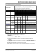
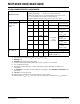
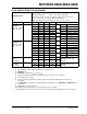
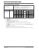
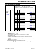
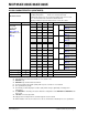
MCP454X/456X/464X/466X PRODUCT IDENTIFICATION SYSTEM To order or obtain information, e.g., on pricing or delivery, refer to the factory or the listed sales office. PART NO.
MCP454X/456X/464X/466X NOTES: DS22107B-page 100 2008-2013 Microchip Technology Inc.
Note the following details of the code protection feature on Microchip devices: • Microchip products meet the specification contained in their particular Microchip Data Sheet. • Microchip believes that its family of products is one of the most secure families of its kind on the market today, when used in the intended manner and under normal conditions. • There are dishonest and possibly illegal methods used to breach the code protection feature.
Worldwide Sales and Service AMERICAS ASIA/PACIFIC ASIA/PACIFIC EUROPE Corporate Office 2355 West Chandler Blvd. Chandler, AZ 85224-6199 Tel: 480-792-7200 Fax: 480-792-7277 Technical Support: http://www.microchip.com/ support Web Address: www.microchip.