MCP4706/4716/4726 8-/10-/12-Bit Voltage Output Digital-to-Analog Converter with EEPROM and I2C™ Interface Features: • Output Voltage Resolutions: - 12-bit: MCP4726 - 10-bit: MCP4716 - 8-bit: MCP4706 • Rail-to-Rail Output • Fast Settling Time of 6 µs (typical) • DAC Voltage Reference Options: - VDD - VREF Pin • Output Gain Options: - Unity (1x) - 2x, only when VREF pin is used as voltage source • Nonvolatile Memory (EEPROM): - Auto Recall of Saved DAC register setting - Auto Recall of Saved Device Configurat
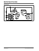
MCP4706/4716/4726 Block Diagram VREF PD1:PD0 SCL DS22272C-page 2 DAC Register EEPROM Control Logic Resistor Ladder SDA I2C™ Interface Logic Buffer VOUT Op Amp PD1:PD0 VW 640 kΩ VSS 125 kΩ VDD Gain (1x or 2x) (G = 0 or 1) VRL 1 kΩ VDD Reference Selection VREF1:VREF0 © 2011-2012 Microchip Technology Inc.
MCP4706/4716/4726 1.0 ELECTRICAL CHARACTERISTICS Absolute Maximum Ratings † Voltage on VDD with respect to VSS .......................................................................................................... -0.6V to +6.5V Voltage on all pins with respect to VSS ..............................................................................................-0.3V to VDD + 0.3V Input clamp current, IIK (VI < 0, VI > VDD) ...............................................................................
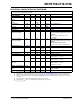
MCP4706/4716/4726 ELECTRICAL CHARACTERISTICS Electrical Specifications: Unless otherwise indicated, VDD = 2.7V to 5.5V, VSS = 0V, RL = 5 kΩ from VOUT to GND, CL = 100 pF, TA = -40°C to +125°C. Typical values at +25°C. Parameters Power Requirements Input Voltage Input Current Symbol Min Typical Max Units VDD IDD 2.7 — — 210 5.5 400 V µA — 210 400 µA Power-Down Current IDDP — 0.09 2 µA Power-On Reset Threshold Power-Up Ramp Rate DC Accuracy Offset Error VPOR — 2.
MCP4706/4716/4726 ELECTRICAL CHARACTERISTICS (CONTINUED) Electrical Specifications: Unless otherwise indicated, VDD = 2.7V to 5.5V, VSS = 0V, RL = 5 kΩ from VOUT to GND, CL = 100 pF, TA = -40°C to +125°C. Typical values at +25°C. Parameters Output Amplifier Minimum Output Voltage Maximum Output Voltage Phase Margin Slew Rate Short Circuit Current Settling Time Power-Down Output Disable Time Delay Power-Down Output Enable Time Delay Symbol Min Typical Max Units VOUT(MIN) — 0.
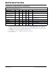
MCP4706/4716/4726 ELECTRICAL CHARACTERISTICS (CONTINUED) Electrical Specifications: Unless otherwise indicated, VDD = 2.7V to 5.5V, VSS = 0V, RL = 5 kΩ from VOUT to GND, CL = 100 pF, TA = -40°C to +125°C. Typical values at +25°C. Parameters Digital Interface Output Low Voltage Input High Voltage (SDA and SCL Pins) Input Low Voltage (SDA and SCL Pins) Input Leakage Pin Capacitance EEPROM EEPROM Write Time Data Retention Endurance Note 1: 2: 3: 4: 5: 6: 7: Symbol Min Typical Max Units VOL VIH — 0.
MCP4706/4716/4726 I2C Mode Timing Waveforms and Requirements 1.1 VPOR (VBOR) VDD tPORD SCL tBORD VIH VIH SDA VOUT pulled down by internal 500 kΩ (typical) resistor VOUT I2C™ Interface is operational FIGURE 1-1: Power-On and Brown-Out Reset Waveforms. Stop ACK Start ACK SDA SCL tPDE tPDD VOUT I2C Power-Down Command Timing.
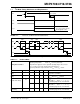
MCP4706/4716/4726 VIH SCL 93 91 90 92 111 SDA VIL Start Condition Stop Condition I2C Bus Start/Stop Bits Timing Waveforms. FIGURE 1-3: I2C BUS START/STOP BITS REQUIREMENTS TABLE 1-2: I2C™ AC Characteristics Param. Symbol No.
MCP4706/4716/4726 103 102 100 101 SCL 90 106 91 92 107 SDA In 110 109 109 SDA Out I2C Bus Data Timing. FIGURE 1-4: TABLE 1-3: I2C BUS DATA REQUIREMENTS (SLAVE MODE) I2C™ AC Characteristics Param. No.
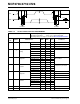
MCP4706/4716/4726 I2C BUS DATA REQUIREMENTS (SLAVE MODE) (CONTINUED) TABLE 1-3: I2C™ AC Characteristics Param. No.
MCP4706/4716/4726 TABLE 1-3: I2C BUS DATA REQUIREMENTS (SLAVE MODE) (CONTINUED) I2C™ AC Characteristics Param. No.
MCP4706/4716/4726 I2C BUS DATA REQUIREMENTS (SLAVE MODE) (CONTINUED) TABLE 1-3: I2C™ AC Characteristics Param. No. Sym Characteristic 111 TSP Input filter spike suppression (SDA and SCL) Note 1: 2: 3: 4: 5: 6: 7: 8: Standard Operating Conditions (unless otherwise specified) Operating Temperature -40°C ≤ TA ≤ +125°C (Extended) Operating Voltage VDD range is described in Electrical Characteristics Min Max Units Conditions 100 kHz mode — 50 ns 400 kHz mode — 50 ns 1.
MCP4706/4716/4726 TEMPERATURE CHARACTERISTICS Electrical Specifications: Unless otherwise indicated, VDD = +2.7V to +5.5V, VSS = GND.
MCP4706/4716/4726 NOTES: DS22272C-page 14 © 2011-2012 Microchip Technology Inc.
MCP4706/4716/4726 2.0 TYPICAL PERFORMANCE CURVES Note: The graphs and tables provided following this note are a statistical summary based on a limited number of samples and are provided for informational purposes only. The performance characteristics listed herein are not tested or guaranteed. In some graphs or tables, the data presented may be outside the specified operating range (e.g., outside specified power supply range) and therefore outside the warranted range.
MCP4706/4716/4726 0.4 0.4 0.3 0.3 0.2 0.2 DNL Error (LSb) DNL Error (LSb) Note: Unless otherwise indicated, TA = +25°C, VDD = 5V, VSS = 0V, VRL = Internal, Gain = x1, RL = 5 kΩ, CL = 100 pF. 0.1 0.0 -0.1 -0.2 0.1 0.0 -0.1 -0.2 -40C +25C +85C +125C -0.3 -40C +25C +85C +125C -0.3 -0.4 -0.4 0 1024 2048 3072 4096 0 1024 Volatile DAC Register Code 0.3 0.3 0.2 0.2 0.1 0.1 0.0 -0.1 -40C +25C +85C +125C 4096 0.0 -0.1 -40C +25C +85C +125C -0.2 -0.3 -0.
MCP4706/4716/4726 Note: Unless otherwise indicated, TA = +25°C, VDD = 5V, VSS = 0V, VRL = Internal, Gain = x1, RL = 5 kΩ, CL = 100 pF. -18.0 2.7V 5.0V 5.5V -20.0 Full Scale Error (LSb) Zero Scale Error (LSb) 2.0 1.5 1.0 0.5 -22.0 -24.0 -26.0 -28.0 2.7V 5.0V 5.5V -30.0 0.0 -32.0 -40 -20 0 20 40 60 80 100 120 -40 -20 0 20 Temperature (°C) FIGURE 2-13: Zero-Scale Error (ZSE) vs. VDD and Temperature (MCP4726). VREF1:VREF0 = 00. 80 100 120 -4.0 2.7V 5.0V 5.5V 0.4 0.3 0.2 -5.
MCP4706/4716/4726 Note: Unless otherwise indicated, TA = +25°C, VDD = 5V, VSS = 0V, VRL = Internal, Gain = x1, RL = 5 kΩ, CL = 100 pF. 12 12 -40C +25C +85C +125C 8 4 INL Error (LSb) INL Error (LSb) 8 -40C +25C +85C +125C 0 -4 -8 4 0 -4 -8 -12 -12 0 1024 2048 3072 4096 0 1024 Volatile DAC Register Code FIGURE 2-19: INL vs. Code (code = 100 to 4000) and Temperature (MCP4726). VDD = 5V, VREF1:VREF0 = 10, G = 0, VREF = VDD.
MCP4706/4716/4726 0.4 0.4 0.3 0.3 0.2 0.2 DNL Error (LSb) DNL Error (LSb) Note: Unless otherwise indicated, TA = +25°C, VDD = 5V, VSS = 0V, VRL = Internal, Gain = x1, RL = 5 kΩ, CL = 100 pF. 0.1 0.0 -0.1 -0.2 0.1 0.0 -0.1 -0.2 -40C +25C +85C +125C -0.3 -40C +25C +85C +125C -0.3 -0.4 -0.4 0 1024 2048 3072 4096 0 1024 Volatile DAC Register Code 0.3 0.3 0.2 0.2 0.1 0.1 0.0 -0.1 -40C +25C +85C +125C 4096 0.0 -0.1 -40C +25C +85C +125C -0.2 -0.3 -0.
MCP4706/4716/4726 Note: Unless otherwise indicated, TA = +25°C, VDD = 5V, VSS = 0V, VRL = Internal, Gain = x1, RL = 5 kΩ, CL = 100 pF. -18.0 2.7V 5.0V 5.5V -20.0 Full Scale Error (LSb) Zero Scale Error (LSb) 2.0 1.5 1.0 0.5 -22.0 -24.0 -26.0 -28.0 2.7V 5.0V 5.5V -30.0 0.0 -32.0 -40 -20 0 20 40 60 80 100 120 -40 -20 0 20 Temperature (°C) FIGURE 2-31: Zero-Scale Error (ZSE) vs. Temperature (MCP4726). VDD = 5V, VREF1:VREF0 = 10, G = 0, VREF = VDD. 80 100 120 -4.0 2.7V 5.0V 5.
MCP4706/4716/4726 Note: Unless otherwise indicated, TA = +25°C, VDD = 5V, VSS = 0V, VRL = Internal, Gain = x1, RL = 5 kΩ, CL = 100 pF. 12 12 -40C +25C +85C +125C 8 4 INL Error (LSb) INL Error (LSb) 8 -40C +25C +85C +125C 0 -4 -8 4 0 -4 -8 -12 -12 0 1024 2048 3072 4096 0 1024 Volatile DAC Register Code FIGURE 2-37: INL vs. Code (code = 100 to 4000) and Temperature (MCP4726). VDD = 5V, VREF1:VREF0 = 11, G = 0, VREF = VDD.
MCP4706/4716/4726 0.4 0.4 0.3 0.3 0.2 0.2 DNL Error (LSb) DNL Error (LSb) Note: Unless otherwise indicated, TA = +25°C, VDD = 5V, VSS = 0V, VRL = Internal, Gain = x1, RL = 5 kΩ, CL = 100 pF. 0.1 0.0 -0.1 -0.2 0.1 0.0 -0.1 -0.2 -40C +25C +85C +125C -0.3 -40C +25C +85C +125C -0.3 -0.4 -0.4 0 1024 2048 3072 4096 0 1024 Volatile DAC Register Code 0.3 0.3 0.2 0.2 0.1 0.1 0.0 -0.1 -40C +25C +85C +125C 4096 0.0 -0.1 -40C +25C +85C +125C -0.2 -0.3 -0.
MCP4706/4716/4726 Note: Unless otherwise indicated, TA = +25°C, VDD = 5V, VSS = 0V, VRL = Internal, Gain = x1, RL = 5 kΩ, CL = 100 pF. -18.0 2.7V 5.0V 5.5V -20.0 Full Scale Error (LSb) Zero Scale Error (LSb) 2.0 1.5 1.0 0.5 -22.0 -24.0 -26.0 -28.0 2.7V 5.0V 5.5V -30.0 0.0 -32.0 -40 -20 0 20 40 60 80 100 120 -40 -20 0 20 Temperature (°C) FIGURE 2-49: Zero-Scale Error (ZSE) vs. Temperature (MCP4726). VDD = 5V, VREF1:VREF0 = 11, G = 0, VREF = VDD. 80 100 120 -4.0 2.7V 5.0V 5.
MCP4706/4716/4726 Note: Unless otherwise indicated, TA = +25°C, VDD = 5V, VSS = 0V, VRL = Internal, Gain = x1, RL = 5 kΩ, CL = 100 pF. 16 0.5 2.7V 5.0V 5.5V 0.4 0.3 0.2 8 DNL Error (LSb) INL Error (LSb) 12 4 0 0.1 0.0 -0.1 -0.2 -0.3 -4 2.7V 5.0V 5.5V -0.4 -8 -0.5 0 1024 2048 3072 0 4096 1024 Volatile DAC Register Code FIGURE 2-55: INL vs. Code (code = 100 to 4000) and VDD (2.7V, 5V, 5.5V) (MCP4726). VREF1:VREF0 = 10, G = 1, VREF = VDD/2, Temp = +25°C.
MCP4706/4716/4726 Note: Unless otherwise indicated, TA = +25°C, VDD = 5V, VSS = 0V, VRL = Internal, Gain = x1, RL = 5 kΩ, CL = 100 pF. 16 0.5 2.7V 5.0V 5.5V 0.4 0.3 0.2 8 DNL Error (LSb) INL Error (LSb) 12 4 0 0.1 0.0 -0.1 -0.2 -0.3 -4 2.7V 5.0V 5.5V -0.4 -8 -0.5 0 1024 2048 3072 0 4096 1024 Volatile DAC Register Code FIGURE 2-61: INL vs. Code (code = 100 to 4000) and VDD (2.7V, 5V, 5.5V) (MCP4726). VREF1:VREF0 = 11, G = 1, VREF = VDD/2, Temp = +25°C.
MCP4706/4716/4726 Note: Unless otherwise indicated, TA = +25°C, VDD = 5V, VSS = 0V, VRL = Internal, Gain = x1, RL = 5 kΩ, CL = 100 pF. 1.0 16 1V 2V 3V 4V 5V 2V 5V 3V 0.5 8 DNL Error (LSb) INL Error (LSb) 12 1V 4V 4 0 0.0 -0.5 -4 -8 -1.0 0 1024 2048 3072 0 4096 1024 Volatile DAC Register Code FIGURE 2-67: INL vs. Code (code = 100 to 4000) and VREF (MCP4726). VDD = 5V, VREF1:VREF0 = 10, G = 0, VREF = 1V, 2V, 3V, 4V, and 5V, Temp = +25°C. 0.5 1V 2V 3V 4V 5V 1V 4V 0.
MCP4706/4716/4726 Note: Unless otherwise indicated, TA = +25°C, VDD = 5V, VSS = 0V, VRL = Internal, Gain = x1, RL = 5 kΩ, CL = 100 pF. 1.0 16 1V 2V 3V 4V 5V 2V 5V 3V 0.5 8 DNL Error (LSb) INL Error (LSb) 12 1V 4V 4 0 0.0 -0.5 -4 -8 -1.0 0 1024 2048 3072 0 4096 1024 Volatile DAC Register Code FIGURE 2-73: INL vs. Code (code = 100 to 4000) and VREF (MCP4726). VDD = 5V, VREF1:VREF0 = 11, G = 0, VREF = 1V, 2V, 3V, 4V, and 5V, Temp = +25°C. 0.5 1V 2V 3V 4V 5V 1V 4V 0.
MCP4706/4716/4726 Note: Unless otherwise indicated, TA = +25°C, VDD = 5V, VSS = 0V, VRL = Internal, Gain = x1, RL = 5 kΩ, CL = 100 pF. -20.0 2.7V 5.0V 5.5V -22.0 Output Error (LSb) -22.0 Output Error (LSb) -20.0 2.7V 5.0V 5.5V -24.0 -26.0 -28.0 -30.0 -24.0 -26.0 -28.0 -30.0 -32.0 -32.0 -34.0 -34.0 -36.0 -36.0 -40 -20 0 20 40 60 80 100 120 -40 -20 0 20 FIGURE 2-79: Output Error vs. Temperature (MCP4726). VDD = 2.7V and 5V, VREF1:VREF0 = 00, Code = 4000.
MCP4706/4716/4726 Note: Unless otherwise indicated, TA = +25°C, VDD = 5V, VSS = 0V, VRL = Internal, Gain = x1, RL = 5 kΩ, CL = 100 pF. -20.0 2.7V 5.0V 5.5V Output Error (LSb) -22.0 -24.0 -26.0 -28.0 -30.0 -32.0 -34.0 -36.0 -40 -20 0 20 40 60 80 100 120 Temperature (°C) FIGURE 2-85: Output Error vs. Temperature (MCP4726). VDD = 2.7V and 5V, VREF1:VREF0 = 11, G = 0, VREF = VDD, Code = 4000. Output Error (LSb) -4.0 2.7V 5.0V 5.5V -5.0 -6.0 -7.0 -8.
MCP4706/4716/4726 Note: Unless otherwise indicated, TA = +25°C, VDD = 5V, VSS = 0V, VRL = Internal, Gain = x1, RL = 5 kΩ, CL = 100 pF. 250 500 2.7V 3.3V 4.5V 5.0V 5.5V 225 2.7V 3.3V 4.5V 5.0V 5.5V 400 IPowerDown (nA) IDD (uA) 200 175 150 300 200 100 125 100 0 -40 -20 0 20 40 60 80 100 120 Temperature (°C) -40 -20 0 20 40 60 80 100 120 Temperature (°C) FIGURE 2-88: IDD vs. Temperature. VDD = 2.7V and 5V, VREF1:VREF0 = 00. FIGURE 2-91: Power-down Current vs. Temperature.
MCP4706/4716/4726 Note: Unless otherwise indicated, TA = +25°C, VDD = 5V, VSS = 0V, VRL = Internal, Gain = x1, RL = 5 kΩ, CL = 100 pF. 70 6 Code = FFFh 2.7V 5.0V 5.5V 5 VOUT (V) VIH (% VDD) 65 60 4 3 2 55 1 0 50 -40 -20 0 20 40 60 80 100 0 120 Temperature (°C) FIGURE 2-92: VIH Threshold of SDA/SCL Inputs vs. Temperature and VDD. 1000 2000 3000 4000 Load Resistance (RL) (:) FIGURE 2-94: VDD = 5.0V. 50 5000 VOUT vs. Resistive Load. 6 Code = FFFh 2.7V 5.0V 5.
MCP4706/4716/4726 Note: Unless otherwise indicated, TA = +25°C, VDD = 5V, VSS = 0V, VREF = Internal, Gain = x1, RL = 5 kΩ, CL = 100 pF. FIGURE 2-96: Full-Scale Settling Time (000h to FFFh) (MCP4726). FIGURE 2-98: Half-Scale Settling Time (400h to C00h) (MCP4726). FIGURE 2-97: Full-Scale Settling Time (FFFh to 000h) (MCP4726). FIGURE 2-99: Half-Scale Settling Time (C00h to 400h) (MCP4726). FIGURE 2-100: Exiting Power-Down Mode (MCP4726, Volatile DAC Register = FFFh).
MCP4706/4716/4726 3.0 PIN DESCRIPTIONS An overview of the pin functions are described in Section 3.1 “Analog Output Voltage Pin (VOUT)” through Section 3.7 “Exposed Pad (EP)”. The descriptions of the pins are listed in Table 3-1.
MCP4706/4716/4726 3.1 Analog Output Voltage Pin (VOUT) 3.5 Serial Clock Pin (SCL) In Normal mode, the DC impedance of the output pin is about 1Ω. In Power-Down mode, the output pin is internally connected to a known pull-down resistor of 1 kΩ, 125 kΩ, or 640 kΩ. The power-down selection bits settings are shown in Table 4-2. SCL is the serial clock pin of the I2C interface. The MCP47X6 devices act only as a slave and the SCL pin accepts only external serial clocks.
MCP4706/4716/4726 4.0 GENERAL DESCRIPTION 4.1 The MCP4706, MCP4716, and MCP4726 devices are single channel voltage output 8-bit, 10-bit, and 12-bit DAC devices with nonvolatile memory (EEPROM) and an I2C serial interface. This family will be referred to as MCP47X6. The devices use a resistor ladder architecture. The resistor ladder DAC is driven from a software selectable voltage reference source. The source can be either the device’s internal VDD or the external VREF pin voltage.
MCP4706/4716/4726 4.2 DAC’s (Resistor Ladder) Reference Voltage The device can be configured to use one of three voltage sources for the resistor ladder’s reference voltage (VRL) (see Figure 4-2). These are: 1. 2. 3. VDD pin voltage VREF pin voltage internally buffered VREF pin voltage unbuffered The selection of the voltage is specified with the volatile VREF1:VREF0 Configuration bits (see Table 4-4). There are nonvolatile and volatile VREF1:VREF0 Configuration bits.
MCP4706/4716/4726 4.4 Output Buffer/VOUT Operation The DAC output is buffered with a low power and precision output amplifier (op amp). Figure 4-4 shows a block diagram. This amplifier provides a rail-to-rail output with low offset voltage and low noise. The user can select the output gain of the output amplifier. Gain options are: a) b) Gain of 1, with either VDD or VREF pin used as reference voltage Gain of 2, only when VREF pin is used as reference voltage.
MCP4706/4716/4726 4.4.3 OUTPUT SLEW RATE Figure 4-5 shows an example of the slew rate of the VOUT pin. The slew rate can be affected by the characteristics of the circuit connected to the VOUT pin. VOUT(B) Wiper = A Wiper = B Time Slew Rate = FIGURE 4-5: 4.4.4 | VOUT(B) - VOUT(A) | ΔT VOUT pin Slew Rate. SMALL CAPACITIVE LOAD With a small capacitive load, the output buffer’s current is not affected by the capacitive load (CL).
MCP4706/4716/4726 TABLE 4-1: Device DAC INPUT CODE VS. ANALOG OUTPUT (VOUT) (VDD = 5.0V) Volatile DAC Register Value LSb VRL 5.0V 1111 1111 1111 0111 1111 1111 MCP4726 (12-bit) 0011 1111 1111 0000 0000 0000 11 1111 1111 01 1111 1111 MCP4716 (10-bit) 00 1111 1111 00 0000 0000 1111 1111 0111 1111 MCP4706 (8-bit) 0011 1111 0000 0000 Note 1: 2: 3: 4: Gain Selection (1) VOUT (4) Equation uV (2) 5.0V/4096 1,220.7 1x VRL * (4095/4096) * 1 4.998779 1x VRL * (4095/4096) * 1 2.
MCP4706/4716/4726 Power-Down Operation Gain (1x or 2x) (Gx = 0 or 1) To allow the application to conserve power when the DAC operation is not required, three Power-Down modes are available. The Power-Down Configuration bits (PD1:PD0) control the power-down operation (Figure 4-7). All Power-Down modes do the following: VW Depending on the selected Power-Down mode, the following will occur: FIGURE 4-7: Diagram.
MCP4706/4716/4726 4.6 Device Resets 4.7 Device Resets can be grouped into two types: Resets due to change in voltage (POR/BOR Reset), and Resets caused by the system master (such as a microcontroller). The MCP47X6 devices have both volatile and nonvolatile (EEPROM) memory. Figure 4-8 shows the volatile and nonvolatile memory and their interaction due to a POR event. After a device Reset, and when VDD ≥ VDD(MIN), the device memory may be written or read. 4.6.
MCP4706/4716/4726 TABLE 4-3: STATUS BITS OPERATION Name Function This bit indicates the state of the EEPROM program memory 1 = EEPROM is not in a programming cycle 0 = EEPROM is in a programming cycle RDY/BSY POR Power-on Reset Status Indicator (flag) 1 = Device is powered on with VDD > VPOR. Ensure that VDD is above VDD(MIN) to ensure proper operation. 0 = Device is in powered off state. If this value is read, VDD < VDD(MIN) < VPOR. Unreliable device operation should be expected.
MCP4706/4716/4726 I2C SERIAL INTERFACE 5.0 The MCP47X6 devices support the I2C serial protocol. The MCP47X6 I2C’s module operates in Slave mode (does not generate the serial clock). 5.1 5.2 Signal Descriptions The I2C interface uses up to two pins (signals). These are: • SDA (Serial Data) • SCL (Serial Clock) Overview 2 This I C interface is a two-wire interface. Figure 5-1 shows a typical I2C interface connection. The I2C interface specifies different communication bit rates.
MCP4706/4716/4726 5.3 I2C Operation 5.3.1.3 The MCP47X6’s I2C module is compatible with the NXP I2C specification. The following lists some of the module’s features: • 7-bit slave addressing • Supports three clock rate modes: - Standard mode, clock rates up to 100 kHz - Fast mode, clock rates up to 400 kHz - High-speed mode (HS mode), clock rates up to 3.4 MHz • Support multi-master applications • General call addressing (Reset and Wake-Up commands) The I2C 10-bit Addressing mode is not supported.
MCP4706/4716/4726 5.3.1.4 5.3.1.5 Repeated Start Bit The Repeated Start bit (see Figure 5-5) indicates the current master device wishes to continue communicating with the current slave device without releasing the I2C bus. The Repeated Start condition is the same as the Start condition, except that the Repeated Start bit follows a Start bit (with the Data bits + A bit) and not a Stop bit. Stop Bit The Stop bit (see Figure 5-6) Indicates the end of the I2C Data Transfer Sequence.
MCP4706/4716/4726 5.3.4 SLOPE CONTROL TABLE 5-2: I2C ADDRESS/ORDER CODE The MCP47X6 implements slope control on the SDA output. 7-bit I2C™ Device Order Code Address As the device transitions from HS mode to FS mode, the slope control parameter will change from the HS specification to the FS specification. ‘1100000’ For Fast (FS) and High-Speed (HS) modes, the device has a spike suppression and a Schmidt Trigger at SDA and SCL inputs. ‘1100001’ ‘1100010’ 5.3.
MCP4706/4716/4726 5.3.6 HS MODE After switching to the High-Speed mode, the next transferred byte is the I2C control byte, which specifies the device to communicate with, and any number of data bytes plus acknowledgements. The master device can then either issue a Repeated Start bit to address a different device (at High-Speed) or a Stop bit to return to Fast/Standard bus speed. After the Stop bit, any other master device (in a multi-master system) can arbitrate for the I2C bus.
MCP4706/4716/4726 5.3.7 GENERAL CALL The MCP47X6 has two General Call commands. The function of these commands are: The General Call is a method that the “master” device can communicate with all other “slave” devices. In a multi-master application, the other master devices are operating in Slave mode. The General Call address has two documented formats. These are shown in Figure 5-11.
MCP4706/4716/4726 MCP47X6 I2C COMMANDS 6.0 TABLE 6-1: The I2C protocol does not specify how commands are formatted, so this section specifies the MCP47X6’s I2C command formats and operation. Operation Write Volatile Memory Command The supported commands are shown in Table 6-2. Many of these commands allow for continuous operation. This means that the I2C master does not generate a Stop bit but repeats the required data/clocks.
MCP4706/4716/4726 6.1 Write Volatile DAC Register (C2:C0 = 00x) This command is used to update the volatile DAC register value and the two Power-down Configuration bits (PD1:PD0). This command is typically used for a quick update of the analog output by modifying the minimum parameters. The EEPROM values are not affected by this command. Figure 6-1 shows an example of the command format, where a Stop bit completes the command.
MCP4706/4716/4726 6.2 Write Volatile Memory (C2:C0 = 010) This Write command is used to update the volatile DAC register value and Configuration bits. The EEPROM is not affected by this command. Figure 6-2 shows an example of this Write command. The volatile DAC register and Configuration bits are updated with the written date at the completion of the ACK bit (falling edge of SCL).
MCP4706/4716/4726 6.3 Write All Memory (C2:C0 = 011) Note: This Write command is used to update the volatile and nonvolatile (EEPROM) DAC register value and Configuration bits. Figure 6-3 shows an example of this Write command. • VOUT update: At the falling edge of the Acknowledge pulse of the 4th byte. • EEPROM update: At the falling edge of the Acknowledge pulse of the 4th byte. RDY/BSY bit toggles to “low” and back to “high” after the EEPROM write is completed.
MCP4706/4716/4726 6.4 Write Volatile Configuration Bits (C2:C0 = 100) This Write command is used to update the volatile Configuration register bits only. This command is a quick method to modify the configuration of the DAC, such as the selection of the resistor ladder reference voltage, the op amp gain, and the power-down state. Figure 6-4 shows an example of this Write command.
MCP4706/4716/4726 6.5 READ COMMAND This command reads all the device memory. This includes the volatile and nonvolatile (EEPROM) DAC register values and Configuration bits, and the volatile status bits. This command is executed when the I2C control byte’s Read/Write bit is a ‘1’ (read). This command has two different formats based on the resolution of the device. The 12-bit and 10-bit devices use the format in Figure 6-5, while the 8-bit device uses the format in Figure 6-6.
MCP4706/4716/4726 Read/Write bit (Read) ACK bit (2) Start bit S SDA ACK bit (3) R/W A 1 1 0 0 A2 A1 A0 1 0 VREF1 RDY POR 0 ACK bit (3) A VREF0 PD1 PD0 G 0 A b07 b06 b05 b04 b03 b02 b01 b00 0 SCL Device Addressing Vol. Status bits Vol. Configuration bits Vol. Data bits (8 bits) (3rd byte) ACK/NACK bit (4) Stop bit ACK bit (3) VREF1 RDY POR 1 Vol.
MCP4706/4716/4726 6.6 I2C General Call Commands 6.6.1 GENERAL CALL RESET The device performs General Call Reset if the second byte is “00000110” (06h). At the acknowledgement of this byte, the device will abort the current conversion and perform the following tasks: The device acknowledges the General Call Address command (0x00 in the first byte). The meaning of the general call address is always specified in the second byte. The I2C specification does not allow “00000000” (00h) in the second byte.
MCP4706/4716/4726 6.6.2 GENERAL CALL WAKE-UP This command does not adhere to the I2C specification where if the LSb of the 2nd byte is a ‘1’, it is a ‘Hardware General Call’ (see the NXP I2C Specification). Note: If the second byte is “00001001” (09h), the device forces the volatile power-down bits to ‘00’. The nonvolatile (EEPROM) power-down bit values are not affected by this command. This command allows multiple MCP47X6 devices to wake-up synchronously.
MCP4706/4716/4726 NOTES: DS22272C-page 58 © 2011-2012 Microchip Technology Inc.
MCP4706/4716/4726 7.0 TERMINOLOGY 7.1 Resolution The resolution is the number of DAC output states that divide the full-scale range. For the 12-bit DAC, the resolution is 212, meaning the DAC code ranges from 0 to 4095. 7.2 For a given output voltage range, which is typically the voltage between the Full-Scale voltage and the ZeroScale voltage (VOUT(FS) - VOUT(ZS)), it is divided by the resolution of the device (Equation 7-1).
MCP4706/4716/4726 7.7 Integral Nonlinearity (INL) The Integral Nonlinearity (INL) error is the maximum deviation of an actual transfer function from an ideal transfer function (straight line). In the MCP47X6, INL is calculated using two end points (zero and full scale). INL can be expressed as a percentage of full scale range (FSR) or in a fraction of an LSb. INL is also called relative accuracy. Equation 7-4 shows how to calculate the INL error in LSb and Figure 7-2 shows an example of INL accuracy.
MCP4706/4716/4726 7.9 Gain Error 7.10 The Gain error (see Figure 7-4) is the difference between the actual full-scale output voltage from the ideal output voltage of the DAC transfer curve. The Gain error is calculated after nullifying the Offset error, or Full-Scale error minus the Offset error. The Gain error indicates how well the slope of the actual transfer function matches the slope of the ideal transfer function.
MCP4706/4716/4726 NOTES: DS22272C-page 62 © 2011-2012 Microchip Technology Inc.
MCP4706/4716/4726 TYPICAL APPLICATIONS The MCP47X6 family of devices are general purpose, single channel voltage output DACs for various applications where a precision operation with low-power and nonvolatile EEPROM memory is needed. Since the devices include a nonvolatile EEPROM memory, the user can utilize these devices for applications that require the output to return to the previous set-up value on subsequent power-ups. 8.1.
MCP4706/4716/4726 Power Supply Considerations VDD The power source should be as clean as possible. The power supply to the device is also used for the DAC voltage reference internally if the internal VDD is selected as the resistor ladder’s reference voltage (VREF1:VREF0 = 00 or 01). Analog C3 Output VOUT 1 VSS VDD 2 3 MCP47X6 Any noise induced on the VDD line can affect the DAC performance.
MCP4706/4716/4726 8.3 Application Examples The MCP47X6 devices are rail-to-rail output DACs designed to operate with a VDD range of 2.7V to 5.5V. The internal output op amplifier is robust enough to drive common, small-signal loads directly, thus eliminating the cost and size of external buffers for most applications. The user can use gain of 1 or 2 of the output op amplifier by setting the Configuration register bits. Also, the user can use internal VDD as the reference or use external reference.
MCP4706/4716/4726 8.3.1.2 Building a “Window” DAC 8.4 When calibrating a set point or threshold of a sensor, typically only a small portion of the DAC output range is utilized. If the LSb size is adequate enough to meet the application’s accuracy needs, the unused range is sacrificed without consequences. If greater accuracy is needed, then the output range will need to be reduced to increase the resolution around the desired threshold.
MCP4706/4716/4726 8.5 Selectable Gain and Offset Bipolar Voltage Output In some applications, precision digital control of the output range is desirable. Figure 8-6 illustrates how to use the DAC devices to achieve this in a bipolar or single-supply application. This circuit is typically used for linearizing a sensor whose slope and offset varies. The equation to design a bipolar “window” DAC would be utilized if R3, R4 and R5 are populated. 8.5.
MCP4706/4716/4726 8.6 Designing a Double-Precision DAC 8.7 Building Programmable Current Source Figure 8-7 shows an example design of a single-supply voltage output capable of up to 24-bit resolution. This requires two 12-bit DACs. This design is simply a voltage divider with a buffered output. Figure 8-8 shows an example of building a programmable current source using a voltage follower. The current sensor resistor is used to convert the DAC voltage output into a digitally-selectable current source.
MCP4706/4716/4726 8.8 Serial Interface Communication Times Table 8-1 shows time/frequency of the supported operations of the I2C serial interface for the different serial interface operational frequencies. This, along with the VOUT output performance (such as slew rate), would be used to determine your application’s volatile DAC register update rate.
MCP4706/4716/4726 Software I2C Interface Reset Sequence 8.9 Note: This technique is documented in AN1028. At times, it may become necessary to perform a Software Reset Sequence to ensure the MCP47X6 device is in a correct and known I2C interface state. This technique only resets the I2C state machine. This is useful if the MCP47X6 device powers up in an incorrect state (due to excessive bus noise, etc), or if the master device is reset during communication.
MCP4706/4716/4726 8.10.2 • Power Supply Considerations • Layout Considerations 8.10.1 The typical application will require a bypass capacitor in order to filter high-frequency noise, which can be induced onto the power supply's traces. The bypass capacitor helps to minimize the effect of these noise sources on signal integrity. Figure 8-10 illustrates an appropriate bypass strategy. In this example, the recommended bypass capacitor value is 0.1 µF.
MCP4706/4716/4726 NOTES: DS22272C-page 72 © 2011-2012 Microchip Technology Inc.
MCP4706/4716/4726 9.0 DEVELOPMENT SUPPORT Development support can be classified into two groups. These are: • Development Tools • Technical Documentation 9.1 Development Tools Several development tools are available to assist in your design and evaluation of the MCP47X6 devices. The currently available tools are shown in Table 9-1. These boards may be purchased directly from the Microchip web site at www.microchip.com. 9.1.
MCP4706/4716/4726 9.2 Technical Documentation Several additional technical documents are available to assist you in your design and development. These technical documents include Application Notes, Technical Briefs, and Design Guides. Table 9-2 shows some of these documents.
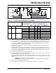
MCP4706/4716/4726 10.0 PACKAGING INFORMATION 10.1 Package Marking Information 6-Lead SOT-23 Example XXNN DC25 PIN 1 PIN 1 Address Option Code MCP4706A0T-E/CH MCP4716A0T-E/CH MCP4726A0T-E/CH A0 (00) DBNN DFNN DKNN A1 (01) DCNN DGNN DLNN A2 (10) DDNN DHNN DMNN A3 (11) DENN DJNN DPNN 6-Lead DFN (2x2x0.
MCP4706/4716/4726 / $ !$ % $ 0 $$ ,33... 3 " .
MCP4706/4716/4726 Note: For the most current package drawings, please see the Microchip Packaging Specification located at http://www.microchip.com/packaging © 2011-2012 Microchip Technology Inc.
MCP4706/4716/4726 DS22272C-page 78 © 2011-2012 Microchip Technology Inc.
MCP4706/4716/4726 © 2011-2012 Microchip Technology Inc.
MCP4706/4716/4726 Note: For the most current package drawings, please see the Microchip Packaging Specification located at http://www.microchip.com/packaging DS22272C-page 80 © 2011-2012 Microchip Technology Inc.
MCP4706/4716/4726 APPENDIX A: REVISION HISTORY Revision C (April 2012) The following is the list of modifications: 1. 2. 3. 4. 5. Updated the layout of the Absolute Maximum Rating page. Added three new sections, Section 4.4.3 “Output Slew Rate”, Section 4.4.4 “Small Capacitive Load” and Section 4.4.5 “Large Capacitive Load”. Enhanced former Section 4.4.3 (now Section 4.4.6 “Driving Resistive and capacitive Loads”).
MCP4706/4716/4726 NOTES: DS22272C-page 82 © 2011-2012 Microchip Technology Inc.
MCP4706/4716/4726 PRODUCT IDENTIFICATION SYSTEM To order or obtain information, e.g., on pricing or delivery, refer to the factory or the listed sales office. X PART NO. XX Device Address Options Device: X Tape and Temperature Reel Range /XX Package MCP4706: Single Channel 8-Bit DAC with EEPROM Memory MCP4716: Single Channel 10-Bit DAC with EEPROM Memory MCP4726: Single Channel 12-Bit DAC with EEPROM Memory A0 = “1100000” I2C Address.
MCP4706/4716/4726 NOTES: DS22272C-page 84 © 2011-2012 Microchip Technology Inc.
Note the following details of the code protection feature on Microchip devices: • Microchip products meet the specification contained in their particular Microchip Data Sheet. • Microchip believes that its family of products is one of the most secure families of its kind on the market today, when used in the intended manner and under normal conditions. • There are dishonest and possibly illegal methods used to breach the code protection feature.
Worldwide Sales and Service AMERICAS ASIA/PACIFIC ASIA/PACIFIC EUROPE Corporate Office 2355 West Chandler Blvd. Chandler, AZ 85224-6199 Tel: 480-792-7200 Fax: 480-792-7277 Technical Support: http://www.microchip.com/ support Web Address: www.microchip.