MCP4728 12-Bit, Quad Digital-to-Analog Converter with EEPROM Memory Features Description • 12-Bit Voltage Output DAC with Four Buffered Outputs • On-Board Nonvolatile Memory (EEPROM) for DAC Codes and I2C™ Address Bits • Internal or External Voltage Reference Selection • Output Voltage Range: - Using Internal VREF (2.048V): The MCP4728 device is a quad, 12-bit voltage output Digital-to-Analog Convertor (DAC) with nonvolatile memory (EEPROM).
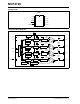
MCP4728 Package Type MCP4728 MSOP VDD 1 10 VSS SCL 2 9 VOUT D SDA 3 8 VOUT C LDAC 4 7 VOUT B RDY/BSY 5 6 VOUT A Functional Block Diagram LDAC EEPROM A VDD INPUT REGISTER A VSS SDA SCL I2C Interface Logic EEPROM B INPUT REGISTER B EEPROM C INPUT REGISTER C EEPROM D RDY/BSY INPUT REGISTER D Internal VREF (2.
MCP4728 1.0 ELECTRICAL CHARACTERISTICS † Notice: Stresses above those listed under “Maximum Absolute Maximum Ratings† VDD...................................................................................6.5V All inputs and outputs w.r.t VSS ................. -0.3V to VDD+0.3V Current at Input Pins ....................................................±2 mA ratings” may cause permanent damage to the device.
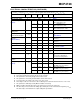
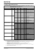
MCP4728 ELECTRICAL CHARACTERISTICS (CONTINUED) Electrical Specifications: Unless otherwise indicated, all parameters apply at VDD = +2.7V to 5.5V, VSS = 0V, RL = 5 kΩ, CL = 100 pF, GX = 1, TA = -40°C to +125°C. Typical values are at +25°C, VIH = VDD, VIL = VSS. Parameter Symbol Min Typical Max Units Conditions Power-on Reset Threshold Voltage VPOR — 2.2 — V All circuits, including EEPROM, are ready to operate.
MCP4728 ELECTRICAL CHARACTERISTICS (CONTINUED) Electrical Specifications: Unless otherwise indicated, all parameters apply at VDD = +2.7V to 5.5V, VSS = 0V, RL = 5 kΩ, CL = 100 pF, GX = 1, TA = -40°C to +125°C. Typical values are at +25°C, VIH = VDD, VIL = VSS. Parameter Symbol Min Typical Max Units Conditions Analog Output (Output Amplifier) Output Voltage Swing VOUT — FSR — V Note 7 Full Scale Range (Note 7) FSR — VDD — V VREF = VDD FSR = from 0.
MCP4728 ELECTRICAL CHARACTERISTICS (CONTINUED) Electrical Specifications: Unless otherwise indicated, all parameters apply at VDD = +2.7V to 5.5V, VSS = 0V, RL = 5 kΩ, CL = 100 pF, GX = 1, TA = -40°C to +125°C. Typical values are at +25°C, VIH = VDD, VIL = VSS.
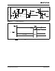
MCP4728 TFSCL TRSCL THIGH TSU:STA SCL TLOW SDA THD:STA TSP THD:DAT 0.7VDD 0.3VDD TAA TFSDA FIGURE 1-1: TSU:STO TBUF TSU:DAT TRSDA I2C Bus Timing Data. LDAC TLDAC 0.7VDD 0.3VDD VOUT (UDAC = 1) No Update FIGURE 1-2: Update LDAC Pin Timing vs. VOUT Update. © 2010 Microchip Technology Inc.
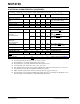
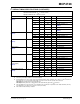
MCP4728 I2C SERIAL TIMING SPECIFICATIONS Electrical Specifications: Unless otherwise specified, all limits are specified for TA = -40 to +125°C, VSS = 0V, Standard and Fast Mode: VDD = +2.7V to +5.5V High Speed Mode: VDD = +4.5V to +5.5V.
MCP4728 I2C SERIAL TIMING SPECIFICATIONS (CONTINUED) Electrical Specifications: Unless otherwise specified, all limits are specified for TA = -40 to +125°C, VSS = 0V, Standard and Fast Mode: VDD = +2.7V to +5.5V High Speed Mode: VDD = +4.5V to +5.5V.
MCP4728 I2C SERIAL TIMING SPECIFICATIONS (CONTINUED) Electrical Specifications: Unless otherwise specified, all limits are specified for TA = -40 to +125°C, VSS = 0V, Standard and Fast Mode: VDD = +2.7V to +5.5V High Speed Mode: VDD = +4.5V to +5.5V. Parameters Bus Free Time (Note 5) Sym Min Typ Max Units TBUF 4700 — — ns Standard Mode 1300 — — ns Fast Mode — — — ns High Speed Mode 1.7 — — — ns High Speed Mode 3.
MCP4728 2.0 TYPICAL PERFORMANCE CURVES Note: The graphs and tables provided following this note are a statistical summary based on a limited number of samples and are provided for informational purposes only. The performance characteristics listed herein are not tested or guaranteed. In some graphs or tables, the data presented may be outside the specified operating range (e.g., outside specified power supply range) and therefore, outside the warranted range.
MCP4728 Note: Unless otherwise indicated, TA = -40°C to +125°C, VDD = +5.0V, VSS = 0V, RL = 5 kΩ, CL = 100 pF. 0.4 VDD = 2.7V, VREF = Internal, Gain = x1 4 0.3 2 0.2 DNL (LSB) INL (LSB) 6 0 -2 0 -0.2 -6 0 1024 2048 Code FIGURE 2-7: 3072 0 4096 INL vs. Code (TA = +25°C). 6 4 0.3 2 0.2 -2 2048 Code 3072 4096 DNL vs. Code (TA = +25°C). 0.4 VDD = 2.7V, VREF = VDD 0 1024 FIGURE 2-10: DNL (LSB) INL (LSB) 0.1 -0.1 -4 VDD = 2.7V, VREF = VDD 0.1 0 -0.1 -4 -0.
MCP4728 Note: Unless otherwise indicated, TA = -40°C to +125°C, VDD = +5.0V, VSS = 0V, RL = 5 kΩ, CL = 100 pF. 0.4 6 V DD = 5.5V, VREF = Internal, Gain = x2 4 o - 40 C o o +25 C +85 C 0.2 DNL (LSB) INL (LSB) 2 0 -2 -4 -8 0 -0.2 o +125 C -10 +125oC - 40oC to +85oC -0.3 0 1024 2048 Code FIGURE 2-13: Temperature. 3072 4096 0 0.5 VDD = 2.7V, VREF = Internal, Gain = x1 4 1024 FIGURE 2-16: Temperature. INL vs. Code and 6 2048 Code 3072 4096 DNL vs. Code and VDD = 2.
MCP4728 Note: Unless otherwise indicated, TA = -40°C to +125°C, VDD = +5.0V, VSS = 0V, RL = 5 kΩ, CL = 100 pF. 0.5 6 VDD = 2.7V, VREF = V DD 4 - 40 oC +85 C 0.3 DNL (LSB) INL (LSB) 2 0 -2 o +125 C -4 0.1 0 -0.2 -8 0 1024 FIGURE 2-19: Temperature. 2048 Code 3072 4096 INL vs. Code and +125oC -0.3 0 - 40oC to +85oC 1024 FIGURE 2-22: Temperature. 2048 Code 3072 4096 DNL vs. Code and 6 -10 VDD = 2.7V, Gain = 1 -20 VDD = 5.
MCP4728 Note: Unless otherwise indicated, TA = -40°C to +125°C, VDD = +5.0V, VSS = 0V, RL = 5 kΩ, CL = 100 pF. 16 VREF = Internal, Gain = x2 2 o Temp = +25 C 14 12 LSB VOUT (2V/Div) Ch. D 10 Ch. A 8 Ch. B 6 Ch. C 4 LDAC 2 Time (2 µs/Div) 0 0 500 FIGURE 2-25: (VDD = 5.5V). 1000 1500 2000 Codes 2500 3000 3500 Absolute DAC Output Error VOUT (2V/Div) LDAC Time (2 µs/Div) FIGURE 2-26: Full Scale Settling Time (VREF = VDD, VDD = 5V, UDAC = 1, Code Change: 000h to FFFh).
MCP4728 Note: Unless otherwise indicated, TA = -40°C to +125°C, VDD = +5.0V, VSS = 0V, RL = 5 kΩ, CL = 100 pF. Discharging Time due to VOUT (1V/Div) internal pull-down resistor (500 kΩ) VOUT (2V/Div) Time (2 µs/Div) LDAC Time (10 µs/Div) CLK FIGURE 2-31: Full Scale Settling Time (VREF = Internal, VDD = 5V, UDAC = 1, Gain = x1, Code Change: FFFh to 000h).
MCP4728 Note: Unless otherwise indicated, TA = -40°C to +125°C, VDD = +5.0V, VSS = 0V, RL = 5 kΩ, CL = 100 pF. Discharging Time due to internal pull-down resistor (500 kΩ) VOUT at Channel D (5V/Div) VOUT (2V/Div) LDAC VOUT at Channel A (100 mV/Div) Time (5 µs/Div) Time (20 µs/Div) CLK Last ACK CLK pulse FIGURE 2-37: Entering Power Down Mode (Code: FFFh, VREF = VDD, VDD = 5V, PD1= PD0 = 1, No External Load). FIGURE 2-40: Channel Cross Talk (VREF = VDD, VDD = 5V).
MCP4728 Note: Unless otherwise indicated, TA = -40°C to +125°C, VDD = +5.0V, VSS = 0V, RL = 5 kΩ, CL = 100 pF. 900 6 5 VDD = 5V VREF = VDD Code = FFFh 3 2 700 VDD = 4.5V VDD = 3.3V 600 VDD = 2.7V 1 500 0 0 1 2 3 Load Resistance (kΩ) FIGURE 2-43: -40 -25 -10 5 600 2 Channels On 400 200 35 50 65 80 95 110 125 VDD = 5.0V All Channels On 800 IDD_INT (µA) 3 Channels On 20 FIGURE 2-46: IDD vs. Temperature (VREF = VDD, All channels are in Normal Mode, Code = FFFh).
MCP4728 Note: Unless otherwise indicated, TA = -40°C to +125°C, VDD = +5.0V, VSS = 0V, RL = 5 kΩ, CL = 100 pF. 900 6 VDD = 5.5V All Channels On Code = FFFh 5 VDD = 5V VDD = 4.5V 700 VDD = 3.3V VOUT (V) IDD_INT (µA) 800 4 3 2 600 1 VDD = 2.7V 500 0 -40 -25 -10 5 20 35 50 65 80 95 110 125 0 2 4 6 o Temperature ( C) FIGURE 2-49: IDD vs. Temperature (VREF = Internal , All Channels are in Normal Mode, Code = FFFh).
MCP4728 NOTES: DS22187E-page 20 © 2010 Microchip Technology Inc.
MCP4728 3.0 PIN DESCRIPTIONS The descriptions of the pins are listed in Table 3-1. TABLE 3-1: Pin No. PIN FUNCTION TABLE Name Pin Type Function 1 VDD P Supply Voltage 2 SCL OI I2C Serial Clock Input (Note 1) 3 SDA OI/OO 4 LDAC ST This pin is used for two purposes: (a) Synchronization Input. It is used to transfer the contents of the DAC input registers to the output registers (VOUT). (b) Select the device for reading and writing I2C address bits.
MCP4728 3.3 Serial Data Pin (SDA) 3.5 SDA is the serial data pin of the I2C interface. The SDA pin is used to write or read the DAC register and EEPROM data. Except for Start and Stop conditions, the data on the SDA pin must be stable during the high duration of the clock pulse. The High or Low state of the SDA pin can only change when the clock signal on the SCL pin is Low. The SDA pin is an open-drain N-channel driver. Therefore, it needs a pull-up resistor from the VDD line to the SDA pin.
MCP4728 4.0 THEORY OF DEVICE OPERATION 4.2 Reset Conditions The device can be reset by two independent events: The MCP4728 device is a 12-bit 4-channel buffered voltage output DAC with nonvolatile memory (EEPROM). The user can program the EEPROM with I2C address bits, configuration and DAC input data of each channel. The device has an internal charge pump circuit to provide the programming voltage of the EEPROM.
MCP4728 4.4 DAC Input Registers and Non-Volatile EEPROM Memory Each channel has its own volatile DAC input register and EEPROM. The details of the input registers and EEPROM are shown in Table 4-1 and Table 4-2, respectively. TABLE 4-1: INPUT REGISTER MAP (VOLATILE) Configuration Bits Bit Name RDY /BSY A2 A1 A0 VREF DAC Input Data (12 bits) DAC1 DAC0 PD1 PD0 GX D11 D10 D9 D8 D7 D6 D5 Ref.
MCP4728 TABLE 4-3: CONFIGURATION BITS Bit Name RDY/BSY (A2, A1, A0) VREF DAC1, DAC0 Functions This is a status indicator (flag) of EEPROM programming activity: 1 = EEPROM is not in programming mode 0 = EEPROM is in programming mode Note: RDY/BSY status can also be monitored at the RDY/BSY pin. Device I2C address bits. See Section 5.3 “MCP4728 Device Addressing” for more details. Voltage Reference Selection bit: 0 = VDD 1 = Internal voltage reference (2.
MCP4728 4.5 Voltage Reference The device has a precision internal voltage reference which provides a nominal voltage of 2.048V. The user can select the internal voltage reference or VDD as the voltage reference source of each channel using the VREF configuration bit. The internal voltage reference circuit is turned off when all channels select VDD as their references. However, it stays turned on if any one of the channels selects the internal reference. 4.6 TABLE 4-4: VREF Internal VREF (2.
MCP4728 TABLE 4-5: LDAC Pin UDAC Bit 0 Update all DAC channel outputs 0 1 Update all DAC channel outputs 1 0 Update a selected DAC channel output 1 1 No update DAC Input Code Vs. DAC Analog Output Table 4-6 shows an example of the DAC input data code vs. analog output. The MSB of the input data is always transmitted first and the format is unipolar binary. DAC Output (VOUT) 0 TABLE 4-6: 4.9 LDAC AND UDAC CONDITIONS VS. OUTPUT UPDATE DAC INPUT CODE VS.
MCP4728 4.10 Normal and Power-Down Modes Each channel has two modes of operation: (a) Normal mode where analog voltage is available and (b) Power-Down mode which turns off most of the internal circuits for power savings. The user can select the operating mode of each channel individually by setting the Power-Down selection bits (PD1 and PD0). For example, the user can select Normal mode for channel A while selecting Power-Down mode for all other channels. See Section 5.
MCP4728 5.0 I2C SERIAL INTERFACE COMMUNICATIONS The MCP4728 device uses a two-wire I2C serial interface. When the device is connected to the I2C bus line, the device works as a slave device. The device supports standard, fast and high speed modes. The following sections describe how to communicate with the MCP4728 device using the I2C serial interface commands. 5.1 Overview of I2C Serial Interface Communications An example of the hardware connection diagram is shown in Figure 7-1.
MCP4728 5.2.5 ACKNOWLEDGE Each receiving device, when addressed, is obliged to generate an acknowledge after the reception of each byte. The master device must generate an extra clock pulse, which is associated with this acknowledge bit. The device that acknowledges has to pull down the SDA line during the acknowledge clock pulse in such a way that the SDA line is stable LOW during the HIGH (A) (B) period of the acknowledge related clock pulse. Of course, setup and hold times must be taken into account.
MCP4728 I2C General Call Commands 5.4 5.4.1 The General Call Reset occurs if the second byte is “00000110” (06h). At the acknowledgement of this byte, the device will abort the current conversion and perform the following tasks: The device acknowledges the general call address command (0x00 in the first byte). The meaning of the general call address is always specified in the second byte. The I2C specification does not allow the use of “00000000” (00h) in the second byte.
MCP4728 5.4.3 GENERAL CALL SOFTWARE UPDATE If the second byte is “00001000” (08h), the device updates all DAC analog outputs (VOUT) at the same time. ACK (MCP4728) Clock Pulse (CLK Line) Start 1 2 3 4 5 Stop 6 7 8 9 1st Byte (General Call Command) 1 2 3 4 5 6 7 8 2nd Byte (Command Type = General Call Software Update) 9 Note 1 Data (SDA Line) Note 1: At this falling edge of the last ACK clock bit, VOUT A, VOUT B, VOUT C, VOUT D are updated.
MCP4728 5.4.4 select the device of interest to read on the I2C bus. The LDAC pin needs a logic transition from “High” to “Low” during the negative pulse of the 8th clock of the second byte, and stays “Low” until the end of the 3rd byte. The maximum clock rate for this command is 400 kHz. GENERAL CALL READ ADDRESS BITS This command is used to read the I2C address bits of the device. If the second byte is “00001100” (0Ch), the device will output its address bits stored in EEPROM and register.
MCP4728 5.5 Writing and Reading Registers and EEPROM 5.6 The Master (MCU) can write or read the DAC input registers or EEPROM using the I2C interface command. The following sections describe the communication examples to write and read the DAC registers and EEPROM using the I2C interface. TABLE 5-1: Table 5-1 summarizes the write command types and their functions.The write command is defined by using three write command type bits (C2, C1, C0) and two write function bits (W1, W0).
MCP4728 5.6.1 FAST WRITE COMMAND (C2=0, C1=0, C0=X, X = DON’T CARE) 5.6.2 MULTI-WRITE COMMAND: WRITE DAC INPUT REGISTERS (C2=0, C1=1, C0=0; W1=0, W0=0) The Fast Write command is used to update the input DAC registers from channels A to D sequentially. The EEPROM data is not affected by this command. This command is called “Fast Write” because it updates the input registers with only limited data bits. Only the Power-Down mode selection bits (PD1 and PD0) and 12 bits of DAC input data are writable.
MCP4728 5.6.3 SEQUENTIAL WRITE COMMAND: WRITE DAC INPUT REGISTERS AND EEPROM SEQUENTIALLY FROM STARTING CHANNEL TO CHANNEL D (C2=0, C1=1, C0=0; W1=1, W0=0) When the device receives this command, it writes the input data to the DAC input registers sequentially from the starting channel to channel D, and also writes to EEPROM sequentially. The starting channel is determined by the DAC1 and DAC0 bits. Table 5-2 shows the functions of the channel selection bits for the sequential write command.
MCP4728 5.6.5 WRITE COMMAND: SELECT VREF BIT (C2=1, C1=0, C0=0) When the device receives this command, it updates the DAC voltage reference selection bit (VREF) of each channel. The EEPROM data is not affected by this command. The affected channel’s analog output is updated after the acknowledge pulse of the last byte. Figure 5-12 shows an example of the write command for Select VREF bits. 5.6.
MCP4728 Command Type Bits: C2=0 C1=0 C0=X ACK (MCP4728) Start S 1st byte 1 1 0 0 2nd Byte (C2 C1) A2 A1 A0 0 A 0 0 PD1 PD0 D11 D10 D9 D8 A D7 D6 D5 D4 D3 D2 D1 D0 A R/W Device Addressing 3rd Byte DAC Input Register of Channel A Fast Write Command Update Channel A DAC Input Register at this ACK pulse. ACK (MCP4728) 3rd Byte 2nd Byte X X PD1 PD0 D11 D10 D9 D8 A D7 D6 D5 D4 D3 D2 D1 D0 A DAC Input Register of Channel B Update Channel B DAC Input Register at this ACK pulse.
MCP4728 Command Type Bits: C2=0 C1=1 C0=0 W1=0 W0=0 ACK (MCP4728) Start 1st byte S 1 1 0 0 A2 A1 A0 0 A R/W Device Addressing ACK (MCP4728) (C2 C1 C0 W1 W2) 0 1 0 0 2nd Byte 3rd Byte 4th Byte 0 DAC1 DAC0 UDAC A VREF PD1 PD0 Gx D11 D10 D9 D8 A D7 D6 D5 D4 D3 D2 D1 D0 A Multi-Write Command Channel Select DAC Input Register of Selected Channel Note 1 Repeat Bytes of the 2nd - 4th Bytes ACK (MCP4728) 2nd byte X X X X Note 3 3rd Byte 4th Byte X DAC1 DAC0 UDAC A VREF PD1 PD0 Gx D1
MCP4728 Command Type Bits: C2=0 C1=1 C0=0 W1=1 W0=0 ACK (MCP4728) Start S 1st byte 1 1 0 0 A2 A1 A0 0 A R/W Device Addressing ACK (MCP4728) 2nd Byte (C2 C1 C0 W1 W2) 0 1 0 1 3rd Byte 4th Byte 0 DAC1 DAC0 UDAC A VREF PD1 PD0 Gx D11 D10 D9 D8 A D7 D6 D5 D4 D3 D2 D1 D0 A Sequential Write Command Sequential Write Starting Channel Select DAC Input Register of Starting Channel Note 1 Repeat Bytes of the 3rd - 4th Bytes for the Starting Channel + 1, ... until Channel D.
MCP4728 Command Type Bits: C2=0 C1=1 C0=0 W1=1 W0=1 ACK (MCP4728) Start S 1st byte 1 1 0 0 A2 A1 A0 0 A R/W Device Addressing ACK (MCP4728) C2 C1 C0 W1 W0 0 1 0 1 Single Write Command Note 1: 2: 2nd Byte 3rd Byte Stop 4th Byte 1 DAC1 DAC0 UDAC A VREF PD1 PD0 Gx D11 D10 D9 D8 A D7 D6 D5 D4 D3 D2 D1 D0 A Channel Select P DAC Input Register of Selected Channel Note 1 and Note 2 VOUT Update: If UDAC = 0 or LDAC Pin = 0: VOUT is updated after the 4th byte’s ACK is issued.
MCP4728 Command Type Bits: Start C2=0 C1=1 (C2 C1 C0) 1st Byte C0=1 2nd Byte S 1 1 0 0 A2 A1 A0 0 A 0 1 1 A2 A1 A0 0 1 A 0 1 1 A2 A1 A0 1 0 A 0 Device Current R/W Command Current Code Address Bits Type Address Bits Stop 4th Byte 3rd Byte New Command Type Address Bits 1 1 A2 A1 A0 1 1 A P Command New Address Bits (for confirmation) Type Note 4 LDAC Pin (Notes 1, 2, 3) Note 3 Clock and LDAC Transition Details: ACK (MCP4728) Clock Pulse (CLK Line) Stop 5 6 7 8 9 1 2 3 4 5 6 3rd
MCP4728 Command Type Bits: C2=1 C1=0 C0=0 ACK (MCP4728) Start S 1st byte 1 1 0 0 A2 A1 A0 0 A 1 0 0 Stop 2nd Byte (C2 C1 C0) X VREF A VREF B VREF C VREF D A P R/W Device Addressing Note 1: 2: Write Command Note 1 Registers and VOUT are updated at this falling edge of ACK pulse. VREF = 0: VDD = 1: Internal Reference (2.
MCP4728 Command Type Bits: C2=1 C1=1 C0=0 ACK (MCP4728) Start S 1st Byte 1 1 0 0 A2 (C2 C1 C0) A1 A0 Device Addressing 0 R/W A 1 1 0 2nd Byte X Write Command for Gain Selection Bits GX A GX B GX C GX D Stop A P Note 1 Registers and VOUT are updated at this falling edge of ACK pulse.
MCP4728 ACK (MCP4728) Read Command Start S 1 1 0 0 A2 A1 A0 1 A R/W Device Code Address Bits ACK (MASTER) 2nd Byte RDY/ BSY POR DAC1 DAC 0 0 3rd Byte A2 A1 A0 A VREF 4th Byte Stop PD1 PD0 GX D11 D10 D9 D8 A D7 D6 D5 D4 D3 D2 D1 D0 A P Channel A DAC Input Register 5th Byte RDY/ BSY POR DAC1 DAC 0 0 6th Byte A2 A1 A0 A VREF 7th Byte Stop PD1 PD0 GX D11 D10 D9 D8 A D7 D6 D5 D4 D3 D2 D1 D0 A P Channel A DAC EEPROM 2nd Byte RDY/ BSY POR DAC1 DAC 0 0 3rd Byte A2 A1 A0 A VREF 4th By
MCP4728 NOTES: DS22187E-page 46 © 2010 Microchip Technology Inc.
MCP4728 6.0 TERMINOLOGY 6.1 Resolution The resolution is the number of DAC output states that divide the full scale range. For the 12-bit DAC, the resolution is 212, meaning the DAC code ranges from 0 to 4095. 6.2 Least Significant Bit (LSB) 7 INL = < -1 LSB 6 INL = - 1 LSB 5 Analog 4 Output (LSB) 3 INL = 0.5 LSB 2 The least significant bit is the ideal voltage difference between two successive codes.
MCP4728 7 DNL = 0.5 LSB 6 5 DNL = 2 LSB Analog 4 Output (LSB) 3 For the MCP4728 device, the gain error is not calibrated at the factory and most of the gain error is contributed by the output buffer (op amp) saturation near the code range beyond 4000. For applications that need the gain error specification less than 1% maximum, a user may consider using the DAC code range between 100 and 4000 instead of using full code range (code 0 to 4095).
MCP4728 6.9 Offset Error Drift Offset error drift is the variation in offset error due to a change in ambient temperature. The offset error drift is typically expressed in ppm/oC. 6.10 Settling Time The Settling time is the time delay required for the DAC output to settle to its new output value from the start of code transition, within specified accuracy. In the MCP4728 device, the settling time is a measure of the time delay until the DAC output reaches its final value within 0.
MCP4728 NOTES: DS22187E-page 50 © 2010 Microchip Technology Inc.
MCP4728 7.0 TYPICAL APPLICATIONS 7.1 The MCP4728 device is a part of Microchip’s latest DAC family with nonvolatile EEPROM memory. The device is a general purpose resistor string DAC intended to be used in applications where a precise and low power DAC, with moderate bandwidth, is required. The SCL, SDA, and RDY/BSY pins of the MCP4728 device are open-drain configurations. These pins require a pull-up resistor, as shown in Figure 7-1.
MCP4728 7.1.1 7.3 DEVICE CONNECTION TEST The user can test the presence of the MCP4728 device on the I2C bus line without performing a data conversion. This test can be achieved by checking an acknowledge response from the MCP4728 device after sending a read or write command. Figure 7-2 shows an example with a read command: Set the R/W bit “High” or “Low” in the address byte. Check the ACK pulse after sending the address byte.
MCP4728 7.6 Application Examples The MCP4728 device is a rail-to-rail output DAC designed to operate with a VDD range of 2.7V to 5.5V. Its output amplifier of each channel is robust enough to drive common, small-signal loads directly, thus eliminating the cost and size of external buffers for most applications. Since each channel has its own configuration bits for selecting the voltage reference, gain, power-down, etc.
MCP4728 VDD Light Comparator 1 RSENSE R1 VTRIP1 R2 0.1 µF VDD Light Comparator 2 RSENSE VDD 0.1 µF 10 µF R1 VTRIP2 R1 R2 R3 R4 R2 VDD 1 10 SCL 2 9 VOUT D SDA 3 MCP4728 0.1 µF VSS 8 VOUT C LDAC 4 7 VOUT B RDY/BSY 5 6 VOUT A VDD Light Analog Outputs Comparator 3 RSENSE R1 VTRIP3 To MCU R2 0.
MCP4728 ACK (MCP4728) Start R/W UDAC VREF GX S 1 1 0 0 0 0 0 0 A 0 1 0 1 0 0 0 0 A 0 0 0 0 1 0 0 0 A 0 0 0 0 0 0 0 0 A 1st Byte Device Addressing for Writing Dn = 211 = 2048 Sequential Write Selecting Command Channel A as Starting Channel Update DAC A Input Register at this ACK pulse. ACK (MCP4728) VREF GX 0 0 0 0 1 1 1 1 A 1 1 1 1 1 1 1 1 A Dn = 4095 Update DAC B Input Register at this ACK pulse.
MCP4728 Start 1st Byte 2nd Byte Stop 3rd Byte S 1 1 0 0 A2 A1 A0 0 A 0 1 1 A2 A1 A0 0 1 A 0 1 1 A2 A1 A0 1 0 A Address Byte Fast Mode Write Command .......
MCP4728 8.0 DEVELOPMENT SUPPORT 8.1 Evaluation & Demonstration Boards The MCP4728 Evaluation Board is available from Microchip Technology Inc. This board works with Microchip’s PICkit™ Serial Analyzer. The user can easily program the DAC input registers and EEPROM using the PICkit Serial Analyzer, and test out the DAC analog output voltages.The PICkit Serial Analyzer uses the PC Graphic User Interface software. Refer to www.microchip.
MCP4728 NOTES: DS22187E-page 58 © 2010 Microchip Technology Inc.
MCP4728 9.0 PACKAGING INFORMATION 9.
MCP4728 1 % & % ! % 2 %% 033))) & &3 " ) 2 ' % 2 $ % % " % D N E E1 NOTE 1 1 2 b e A A2 c φ L A1 L1 4 % & 5 & % 6!&( $ 55 * * 6 6 + . / 7 9 % 2 % " $$ 7 < "% " " 2 7 5 % 8 % " " 2 67 : : + ;+ + : + * < "% . / * , .
MCP4728 10-Lead Plastic Micro Small Outline Package (UN) [MSOP] Note: For the most current package drawings, please see the Microchip Packaging Specification located at http://www.microchip.com/packaging © 2010 Microchip Technology Inc.
MCP4728 NOTES: DS22187E-page 62 © 2010 Microchip Technology Inc.
MCP4728 APPENDIX A: REVISION HISTORY Revision E (October 2010) The following is the list of modifications: 1. 2. 3. Corrected values in I2C Serial Timing Specifications table (SCL Fall Time, SDA Fall Time, Data Hold Time, Output Valid from Clock). Updated the Package Marking Information table in the “Packaging Information” section. Updated the information in the section “Product Identification System”. Revision D (October 2009) The following is the list of modifications: 1. 2. 3. 4. 5.
MCP4728 NOTES: DS22187E-page 64 © 2010 Microchip Technology Inc.
MCP4728 PRODUCT IDENTIFICATION SYSTEM To order or obtain information, e.g., on pricing or delivery, refer to the factory or the listed sales office. PART NO. XX Device Address Options Device: X /XX Tape and Temperature Reel Range MCP4728: Address Options: -X XX Package 12-bit, Quad Digital-to-Analog Convertor with EEPROM memory A2 A1 A0 A0 * = 0 0 0 A1 = 0 0 1 A2 = 0 1 0 A3 = 0 1 1 A4 = 1 0 0 A5 = 1 0 1 A6 = 1 1 0 A7 = 1 1 1 * Default option.
MCP4728 NOTES: DS22187E-page 66 © 2010 Microchip Technology Inc.
Note the following details of the code protection feature on Microchip devices: • Microchip products meet the specification contained in their particular Microchip Data Sheet. • Microchip believes that its family of products is one of the most secure families of its kind on the market today, when used in the intended manner and under normal conditions. • There are dishonest and possibly illegal methods used to breach the code protection feature.
Worldwide Sales and Service AMERICAS ASIA/PACIFIC ASIA/PACIFIC EUROPE Corporate Office 2355 West Chandler Blvd. Chandler, AZ 85224-6199 Tel: 480-792-7200 Fax: 480-792-7277 Technical Support: http://support.microchip.com Web Address: www.microchip.