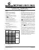
MCP4801/4811/4821 8/10/12-Bit Voltage Output Digital-to-Analog Converter with Internal VREF and SPI Interface Features Description • • • • • • The MCP4801/4811/4821 devices are single channel 8-bit, 10-bit and 12-bit buffered voltage output Digital-to-Analog Converters (DACs), respectively. The devices operate from a single 2.7V to 5.5V supply with an SPI compatible Serial Peripheral Interface. The devices have a high precision internal voltage reference (VREF = 2.048V).
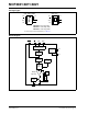
MCP4801/4811/4821 Package Types DFN (2x3)* VDD 1 CS 2 SCK 3 SDI 4 MCP48X1 PDIP, SOIC, MSOP 8 VOUT VDD 1 CS 2 7 VSS 6 SHDN SCK 3 5 LDAC SDI 4 8 VOUT 9 7 VSS 6 SHDN 5 LDAC MCP4801: 8-bit single DAC MCP4811: 10-bit single DAC MCP4821: 12-bit single DAC * Includes Exposed Thermal Pad (EP); see Table 3-1. Block Diagram LDAC CS SDI SCK Interface Logic Power-on Reset Input Register DAC Register VDD VSS VREF (2.
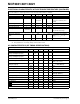
MCP4801/4811/4821 1.0 ELECTRICAL CHARACTERISTICS † Notice: Stresses above those listed under “Maximum Ratings” may cause permanent damage to the device. This is a stress rating only and functional operation of the device at those or any other conditions above those indicated in the operational listings of this specification is not implied. Exposure to maximum rating conditions for extended periods may affect device reliability. Absolute Maximum Ratings † VDD ..............................................
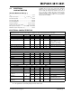
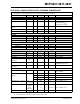
MCP4801/4811/4821 ELECTRICAL CHARACTERISTICS (CONTINUED) Electrical Specifications: Unless otherwise indicated, VDD = 5V, VSS = 0V, VREF = 2.048V, Output Buffer Gain (G) = 2x, RL = 5 k to GND, CL = 100 pF, TA = -40 to +85°C. Typical values are at +25°C. Parameters Sym Min Typ Max Units Conditions 2.008 2.048 2.088 V — 125 325 ppm/°C — 0.25 0.
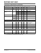
MCP4801/4811/4821 ELECTRICAL CHARACTERISTIC WITH EXTENDED TEMPERATURE Electrical Specifications: Unless otherwise indicated, VDD = 5V, VSS = 0V, VREF = 2.048V, Output Buffer Gain (G) = 2x, RL = 5 k to GND, CL = 100 pF. Typical values are at +125°C by characterization or simulation. Parameters Sym Min Typ Max VDD Units Conditions 2.7 — 5.5 IDD — 350 — µA All digital inputs are grounded, analog output (VOUT) is unloaded. Code = 000h ISHDN — 1.
MCP4801/4811/4821 ELECTRICAL CHARACTERISTIC WITH EXTENDED TEMPERATURE (CONTINUED) Electrical Specifications: Unless otherwise indicated, VDD = 5V, VSS = 0V, VREF = 2.048V, Output Buffer Gain (G) = 2x, RL = 5 k to GND, CL = 100 pF. Typical values are at +125°C by characterization or simulation. Parameters Sym Min Typ Max Units Output Swing VOUT — 0.01 to VDD – 0.
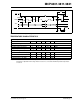
MCP4801/4811/4821 tCSH CS tIDLE tCSSR Mode 1,1 tHI tLO tCHS SCK Mode 0,0 tSU tHD SDI MSb in LSb in LDAC tLS FIGURE 1-1: tLD SPI Input Timing Data. TEMPERATURE CHARACTERISTICS Electrical Specifications: Unless otherwise indicated, VDD = +2.7V to +5.5V, VSS = GND.
MCP4801/4811/4821 2.0 TYPICAL PERFORMANCE CURVES Note: The graphs and tables provided following this note are a statistical summary based on a limited number of samples and are provided for informational purposes only. The performance characteristics listed herein are not tested or guaranteed. In some graphs or tables, the data presented may be outside the specified operating range (e.g., outside specified power supply range) and therefore outside the warranted range.
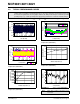
MCP4801/4811/4821 Note: Unless otherwise indicated, TA = +25°C, VDD = 5V, VSS = 0V, VREF = 2.048V, Gain = 2, RL = 5 k, CL = 100 pF. 0.3 0.6 o - 40 C 0.4 0.1 INL (LSB) DNL (LSB) - 40oC 0.5 0.2 0 -0.1 o 85 C 0.3 0.2 0.1 0 125oC -0.1 -0.2 -0.3 -0.3 0 128 256 384 512 640 768 25oC -0.2 +25oC to +125oC 0 896 1024 32 64 96 FIGURE 2-7: DNL vs. Code and Temperature (MCP4811). INL (LSB) Full Scale VOUT (V) 1 85oC 0 -0.5 -1 -1.5 25oC -2 o - 40 C -2.
MCP4801/4811/4821 Note: Unless otherwise indicated, TA = +25°C, VDD = 5V, VSS = 0V, VREF = 2.048V, Gain = 2, RL = 5 k, CL = 100 pF. 10 1E+1 100 1E+2 1k 1E+3 10k 1E+4 FIGURE 2-16: 320 315 310 305 300 IDD Histogram (VDD = 2.7V). 18 1.E-02 10.0 Output Noise Voltage (mV) 16 Occurrence 14 Eni (in VP-P) 0.10 1.E-04 12 10 8 6 4 Eni (in VRMS) 2 FIGURE 2-14: Output Noise Voltage (VREF Noise Voltage) vs. Bandwidth. Gain = 2x.
MCP4801/4811/4821 Note: Unless otherwise indicated, TA = +25°C, VDD = 5V, VSS = 0V, VREF = 2.048V, Gain = 2, RL = 5 k, CL = 100 pF. 0.7 0.4 0.3 0.2 -0.1 VDD -0.15 Gain Error (%) 4.0V 3.0V 2.7V VDD 0.5 ISHDN (µA) -0.05 5.5V 5.0V 0.6 5.5V 5.0V 4.0V 3.0V 2.7V -0.2 -0.25 -0.3 -0.35 -0.4 0.1 -0.45 -0.5 0 -40 -20 0 20 40 60 80 100 -40 120 -20 Ambient Temperature (ºC) FIGURE 2-18: Hardware Shutdown Current vs. Temperature and VDD. 4 20 40 60 80 100 120 5.0V 3 4.0V 2.5 3.0V 2.
MCP4801/4811/4821 Note: Unless otherwise indicated, TA = +25°C, VDD = 5V, VSS = 0V, VREF = 2.048V, Gain = 2, RL = 5 k, CL = 100 pF. 16 2.5 5.5V 2 5.0V 1.75 1.5 4.0V 1.25 1 3.0V 2.7V 0.75 0.5 15 IOUT_HI_SHORTED (mA) VIN_SPI Hysteresis (V) 5.5V 5.0V 4.0V 3.0V 2.7V VDD 2.25 14 VDD 13 12 11 0.25 10 0 -40 -20 0 20 40 60 80 -40 100 120 -20 Ambient Temperature (ºC) FIGURE 2-24: Input Hysteresis vs. Temperature and VDD. 40 60 80 100 120 6.0 4.0V 0.033 0.031 5.0 0.029 4.
MCP4801/4811/4821 Note: Unless otherwise indicated, TA = +25°C, VDD = 5V, VSS = 0V, VREF = 2.048V, Gain = 2, RL = 5 k, CL = 100 pF. VOUT VOUT SCK LDAC LDAC Time (1 µs/div) FIGURE 2-29: VOUT Rise Time. Time (1 µs/div) FIGURE 2-32: VOUT Rise Time. VOUT VOUT SCK SCK LDAC LDAC Time (1 µs/div) VOUT Fall Time. FIGURE 2-33: Shutdown. VOUT Rise Time Exit Ripple Rejection (dB) FIGURE 2-30: Time (1 µs/div) VOUT SCK LDAC Time (1 µs/div) FIGURE 2-31: VOUT Rise Time. 2010 Microchip Technology Inc.
MCP4801/4811/4821 NOTES: DS22244B-page 14 2010 Microchip Technology Inc.
MCP4801/4811/4821 3.0 PIN DESCRIPTIONS The descriptions of the pins are listed in Table 3-1. TABLE 3-1: PIN FUNCTION TABLE FOR MCP4801/4811/4821 MCP4801/4811/4821 Symbol MSOP, PDIP, SOIC, DFN DFN 1 1 3.1 Description VDD Supply Voltage Input (2.7V to 5.5V) 2 2 CS Chip Select Input 3 3 SCK Serial Clock Input 4 4 SDI 5 5 LDAC DAC Output Synchronization Input.
MCP4801/4811/4821 NOTES: DS22244B-page 16 2010 Microchip Technology Inc.
MCP4801/4811/4821 4.0 GENERAL OVERVIEW The MCP4801, MCP4811 and MCP4821 are single channel voltage-output 8-bit, 10-bit and 12-bit DAC devices, respectively. These devices include rail-to-rail output amplifier, internal voltage reference, shutdown and reset-management circuitry. The devices use an SPI serial communication interface and operate with a single supply voltage from 2.7V to 5.5V. The DAC input coding of these devices is straight binary.
MCP4801/4811/4821 4.0.2 DNL ACCURACY 4.1 A Differential Non-Linearity (DNL) error is the measure of the variations in code widths from the ideal code width. A DNL error of zero indicates that every code is exactly 1 LSb wide. 111 110 Actual Transfer Function 101 Digital Input Code 100 Ideal Transfer Function 011 001 Wide Code, >1 LSb 000 Narrow Code, <1 LSb DAC Output 4.0.3 Example for DNL Error.
MCP4801/4811/4821 4.1.3 POWER-ON RESET CIRCUIT The internal Power-on Reset (POR) circuit monitors the power supply voltage (VDD) during the device operation. The circuit also ensures that the DAC powers up with high output impedance ( = 0, typically 500 k. The devices will continue to have a high-impedance output until a valid write command is received, and the LDAC pin meets the input low threshold. If the power supply voltage is less than the POR threshold (VPOR = 2.
MCP4801/4811/4821 NOTES: DS22244B-page 20 2010 Microchip Technology Inc.
MCP4801/4811/4821 5.0 SERIAL INTERFACE 5.1 Overview The MCP4801/4811/4821 devices are designed to interface directly with the Serial Peripheral Interface (SPI) port, available on many microcontrollers, and supports Mode 0,0 and Mode 1,1. Commands and data are sent to the device via the SDI pin, with data being clocked-in on the rising edge of SCK. The communications are unidirectional and, thus, data cannot be read out of the MCP4801/4811/4821 devices.
MCP4801/4811/4821 REGISTER 5-1: WRITE COMMAND REGISTER FOR MCP4821 (12-BIT DAC) W-x W-x W-x W-0 W-x W-x W-x W-x W-x W-x W-x W-x W-x W-x W-x W-x 0 — GA SHDN D11 D10 D9 D8 D7 D6 D5 D4 D3 D2 D1 D0 bit 15 bit 0 REGISTER 5-2: WRITE COMMAND REGISTER FOR MCP4811 (10-BIT DAC) W-x W-x W-x W-0 W-x W-x W-x W-x W-x W-x W-x W-x W-x W-x W-x 0 — GA SHDN D9 D8 D7 D6 D5 D4 D3 D2 D1 D0 x bit 15 W-x x bit 0 REGISTER 5-3: WRITE COMMAND REGISTER FOR MCP4801
MCP4801/4811/4821 CS 0 1 2 3 4 5 6 7 8 9 10 11 12 (Mode 1,1) 13 14 15 SCK (Mode 0,0) config bits 0 SDI 12 data bits — GA SHDN D11 D10 D9 D8 D7 D6 D5 D4 D3 D2 D1 D0 LDAC VOUT FIGURE 5-1: Write Command for MCP4821 (12-bit DAC). CS 0 1 2 3 4 5 6 7 8 9 10 11 12 (Mode 1,1) 13 14 15 SCK (Mode 0,0) config bits 0 SDI 12 data bits — GA SHDN D9 D8 D7 D6 D5 D4 D3 D2 D1 D0 X X LDAC VOUT Note: X = “don’t care” bits. FIGURE 5-2: Write Command for MCP4811 (10-bit DAC).
MCP4801/4811/4821 NOTES: DS22244B-page 24 2010 Microchip Technology Inc.
MCP4801/4811/4821 6.0 TYPICAL APPLICATIONS 6.3 Output Noise Considerations The MCP4801/4811/4821 family of devices are general purpose, single channel voltage output DACs for various applications where a precision operation with low-power and internal voltage reference is required. The voltage noise density (in µV/Hz) is illustrated in Figure 2-13. This noise appears at VOUT, and is primarily a result of the internal reference voltage. Its 1/f corner (fCORNER) is approximately 400 Hz.
MCP4801/4811/4821 6.5 6.5.1.1 Single-Supply Operation Decreasing Output Step Size The MCP4801/4811/4821 devices are rail-to-rail voltage output DAC devices designed to operate with a VDD range of 2.7V to 5.5V. Its output amplifier is robust enough to drive small-signal loads directly. Therefore, it does not require any external output buffer for most applications. If the application is calibrating the bias voltage of a diode or transistor, a bias voltage range of 0.
MCP4801/4811/4821 6.5.1.2 Building a “Window” DAC If the threshold is not near VREF, 2VREF or VSS, then creating a “window” around the threshold has several advantages. One simple method to create this “window” is to use a voltage divider network with a pullup and pull-down resistor. Example 6-2 and Example 6-4 illustrate this concept. When calibrating a set point or threshold of a sensor, typically only a small portion of the DAC output range is utilized.
MCP4801/4811/4821 6.6 Bipolar Operation Example 6-3 illustrates a simple bipolar voltage source configuration. R1 and R2 allow the gain to be selected, while R3 and R4 shift the DAC’s output to a selected offset. Note that R4 can be tied to VDD, instead of VSS, if a higher offset is desired. Also note that a pull-up to VDD could be used instead of R4, or in addition to R4, if a higher offset is desired.
MCP4801/4811/4821 6.7 Selectable Gain and Offset Bipolar Voltage Output This circuit is typically used for linearizing a sensor whose slope and offset varies. The equation to design a bipolar “window” DAC would be utilized if R3, R4 and R5 are populated. In some applications, precision digital control of the output range is desirable. Example 6-4 illustrates how to use the MCP4801/4811/4821 family of devices to achieve this in a bipolar or single-supply application.
MCP4801/4811/4821 6.8 Designing a Double-Precision DAC Step 1: Calculate the resolution needed: Example 6-5 illustrates how to design a single-supply voltage output capable of up to 24-bit resolution by using 12-bit DACs. This design is simply a voltage divider with a buffered output. As an example, if an application similar to the one developed in Section 6.6.
MCP4801/4811/4821 6.9 Building Programmable Current Source However, this also reduces the resolution that the current can be controlled with. The voltage divider, or “window”, DAC configuration would allow the range to be reduced, thus increasing resolution around the range of interest. When working with very small sensor voltages, plan on eliminating the amplifier’s offset error by storing the DAC’s setting under known sensor conditions.
MCP4801/4811/4821 NOTES: DS22244B-page 32 2010 Microchip Technology Inc.
MCP4801/4811/4821 7.0 DEVELOPMENT SUPPORT 7.1 Evaluation & Demonstration Boards The Mixed Signal PICtail™ Demo Board supports the MCP4801/4811/4821 family of devices. Refer to www.microchip.com for further information on this product’s capabilities and availability. 2010 Microchip Technology Inc.
MCP4801/4811/4821 NOTES: DS22244B-page 34 2010 Microchip Technology Inc.
MCP4801/4811/4821 8.0 PACKAGING INFORMATION 8.1 Package Marking Information 8-Lead DFN (2x3) AHS 010 25 XXX YWW NN Example: 8-Lead MSOP XXXXXX YWWNNN 8-Lead PDIP (300 mil) XXXXXXXX XXXXXNNN YYWW Legend: XX...
MCP4801/4811/4821 ' ! "" # $ % & 2 % & % ! % * %% 133))) & &3 " ) * ' % * $ % % " % e D b N N L K E2 E EXPOSED PAD NOTE 1 NOTE 1 2 1 1 2 D2 BOTTOM VIEW TOP VIEW A A3 A1 NOTE 2 4 % & 5 & % 6!&( $ 55 , , 6 6 67 8 9 % . / 0 7 : % 9 % " $$ .
MCP4801/4811/4821 ' ! "" # $ % & 2 % & % ! % * %% 133))) & &3 2010 Microchip Technology Inc.
MCP4801/4811/4821 ' ( )" * + ) % )* & 2 % & % ! % * %% 133))) & &3 " ) * ' % * $ % % " % D N E E1 NOTE 1 1 2 e b A2 A c φ L L1 A1 4 % & 5 & % 6!&( $ 55 , , 6 6 >. / 0 7 : % * % " $$ 7 ; "% " " * 7 5 % 8 9 % " " * 67 < < . 9. . < .
MCP4801/4811/4821 Note: For the most current package drawings, please see the Microchip Packaging Specification located at http://www.microchip.com/packaging 2010 Microchip Technology Inc.
MCP4801/4811/4821 ' ,+ + " # $ % , & 2 % & % ! % * %% 133))) & &3 " ) * ' % * $ % % " % N NOTE 1 E1 1 3 2 D E A2 A L A1 c e eB b1 b 4 % & 5 & % 6!&( $ 60:, 6 6 67 8 9 % / 0 % % < < . + . . < < ! " % ! " ; "% , + + .
MCP4801/4811/4821 ' )" * + ) (( - ! "" # $ %)*, & 2 % & % ! % * %% 133))) & &3 " ) * ' % * $ % % " % D e N E E1 NOTE 1 1 2 3 α h b h A2 A c φ L A1 β L1 4 % & 5 & % 6!&( $ 55 , , 6 6 / 0 7 : % * % " $$ @ 7 ; "% " " * 8 9 % " " * 67 < < . < < < .
MCP4801/4811/4821 ' )" * + ) (( - ! "" # $ %)*, & 2 % & % ! % * %% 133))) & &3 DS22244B-page 42 " ) * ' % * $ % % " % 2010 Microchip Technology Inc.
MCP4801/4811/4821 APPENDIX A: REVISION HISTORY Revision A (April 2010) • Original Release of this Document. Revision B (April 2010) • Corrected the “Related Products” table on page 1. 2010 Microchip Technology Inc.
MCP4801/4811/4821 NOTES: DS22244B-page 44 2010 Microchip Technology Inc.
MCP4801/4811/4821 PRODUCT IDENTIFICATION SYSTEM To order or obtain information, e.g., on pricing or delivery, refer to the factory or the listed sales office. PART NO.
MCP4801/4811/4821 NOTES: DS22244B-page 46 2010 Microchip Technology Inc.
Note the following details of the code protection feature on Microchip devices: • Microchip products meet the specification contained in their particular Microchip Data Sheet. • Microchip believes that its family of products is one of the most secure families of its kind on the market today, when used in the intended manner and under normal conditions. • There are dishonest and possibly illegal methods used to breach the code protection feature.
WORLDWIDE SALES AND SERVICE AMERICAS ASIA/PACIFIC ASIA/PACIFIC EUROPE Corporate Office 2355 West Chandler Blvd. Chandler, AZ 85224-6199 Tel: 480-792-7200 Fax: 480-792-7277 Technical Support: http://support.microchip.com Web Address: www.microchip.