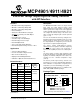
MCP4901/4911/4921 8/10/12-Bit Voltage Output Digital-to-Analog Converter with SPI Interface Features Description • • • • • • The MCP4901/4911/4921 devices are single channel 8-bit, 10-bit and 12-bit buffered voltage output Digital-to-Analog Converters (DACs), respectively. The devices operate from a single 2.7V to 5.5V supply with an SPI compatible Serial Peripheral Interface.
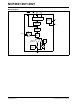
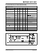
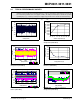
MCP4901/4911/4921 Block Diagram LDAC CS SDI SCK Interface Logic Power-on Reset Input Register VDD VSS DAC Register VREF String DAC Buffer Gain Logic Output Op Amp Output Logic VOUT DS22248A-page 2 2010 Microchip Technology Inc.
MCP4901/4911/4921 1.0 ELECTRICAL CHARACTERISTICS Absolute Maximum Ratings † VDD ............................................................................................................. 6.5V † Notice: Stresses above those listed under “Maximum Ratings” may cause permanent damage to the device. This is a stress rating only and functional operation of the device at those or any other conditions above those indicated in the operational listings of this specification is not implied.
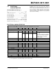
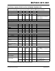
MCP4901/4911/4921 ELECTRICAL CHARACTERISTICS (CONTINUED) Electrical Specifications: Unless otherwise indicated, VDD = 5V, VSS = 0V, VREF = 2.048V, Output Buffer Gain (G) = 2x, RL = 5 k to GND, CL = 100 pF TA = -40 to +85°C. Typical values are at +25°C. Parameters Offset Error Offset Error Temperature Coefficient Sym Min Typ Max Units Conditions VOS — ±0.02 1 % of FSR VOS/°C — 0.16 — ppm/°C -45°C to 25°C +25°C to 85°C Code = 0x000h — -0.44 — ppm/°C gE — -0.
MCP4901/4911/4921 ELECTRICAL CHARACTERISTIC WITH EXTENDED TEMPERATURE Electrical Specifications: Unless otherwise indicated, VDD = 5V, VSS = 0V, VREF = 2.048V, Output Buffer Gain (G) = 2x, RL = 5 k to GND, CL = 100 pF. Typical values are at +125°C by characterization or simulation. Parameters Sym Min Typ Max Units Conditions Input Voltage VDD 2.7 — 5.5 Input Current IDD — 200 — µA VREF input is unbuffered, all digital inputs are grounded, all analog outputs (VOUT) are unloaded.
MCP4901/4911/4921 ELECTRICAL CHARACTERISTIC WITH EXTENDED TEMPERATURE (CONTINUED) Electrical Specifications: Unless otherwise indicated, VDD = 5V, VSS = 0V, VREF = 2.048V, Output Buffer Gain (G) = 2x, RL = 5 k to GND, CL = 100 pF. Typical values are at +125°C by characterization or simulation. Parameters Sym Min Typ Max Units THDVREF — — — dB VREF = 2.5V ±0.1Vp-p, Frequency = 1 kHz Output Swing VOUT — 0.01 to VDD – 0.
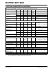
MCP4901/4911/4921 AC CHARACTERISTICS (SPI TIMING SPECIFICATIONS) Electrical Specifications: Unless otherwise indicated, VDD= 2.7V – 5.5V, TA= -40 to +125°C. Typical values are at +25°C. Parameters Sym Min Typ Max Units Schmitt Trigger High Level Input Voltage (All digital input pins) VIH 0.7 VDD — — V Schmitt Trigger Low Level Input Voltage (All digital input pins) VIL — — 0.2 VDD V VHYS — 0.
MCP4901/4911/4921 TEMPERATURE CHARACTERISTICS Electrical Specifications: Unless otherwise indicated, VDD = +2.7V to +5.5V, VSS = GND.
MCP4901/4911/4921 2.0 TYPICAL PERFORMANCE CURVES Note: The graphs and tables provided following this note are a statistical summary based on a limited number of samples and are provided for informational purposes only. The performance characteristics listed herein are not tested or guaranteed. In some graphs or tables, the data presented may be outside the specified operating range (e.g., outside specified power supply range) and therefore outside the warranted range.
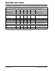
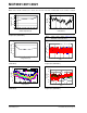
MCP4901/4911/4921 Note: Unless otherwise indicated, TA = +25°C, VDD = 5V, VSS = 0V, VREF = 2.048V, Gain = 2, RL = 5 k, CL = 100 pF. 2 2 0 INL (LSB) Absolute INL (LSB) 2.5 1.5 1 -2 -4 0.5 0 -6 -40 -20 0 20 40 60 80 100 120 0 1024 Ambient Temperature (ºC) 3072 4096 Code (Decimal) FIGURE 2-7: Absolute INL vs. Temperature (MCP4921). FIGURE 2-10: Note: 3 INL vs. Code (MCP4921). Single device graph (Figure 2-10) for illustration of 64 code effect. 0.2 Temp = - 40oC to +125oC 2.5 0.
MCP4901/4911/4921 Note: Unless otherwise indicated, TA = +25°C, VDD = 5V, VSS = 0V, VREF = 2.048V, Gain = 2, RL = 5 k, CL = 100 pF. 0.06 18 Temp = -40oC to +125oC 16 14 Occurrence 0.02 0 -0.02 12 10 8 6 4 2 -0.04 0 32 64 96 128 160 192 224 256 Code 167 165 163 161 159 157 155 153 151 IDD (μA) FIGURE 2-16: 2.7V). FIGURE 2-13: DNL vs. Code and Temperature (MCP4901). 149 147 143 0 -0.06 145 DNL (LSB) 0.04 IDD Histogram (VDD = 9 0.
MCP4901/4911/4921 Note: Unless otherwise indicated, TA = +25°C, VDD = 5V, VSS = 0V, VREF = 2.048V, Gain = 2, RL = 5 k, CL = 100 pF. 6 VDD 4 ISHDN_SW (μA) 5 5.0V 4 4.0V 3 3.0V 2.7V 2 VDD 1 VIN Hi Threshold (V) 5.5V 5.0V 3 2.5 4.0V 2 3.0V 2.7V 1.5 1 0 -40 -20 -40 0 20 40 60 80 100 120 Ambient Temperature (ºC) -20 0 20 40 60 80 100 120 Ambient Temperature (ºC) FIGURE 2-21: VIN High Threshold vs. Temperature and VDD. FIGURE 2-18: Shutdown Current vs. Temperature and VDD. 0.12 0.
MCP4901/4911/4921 VDD 5.5V 5.0V 4.0V 3.0V 2.7V 0.0045 VOUT_LOW Limit (Y-AVSS)(V) 2.5 2.25 2 1.75 1.5 1.25 1 0.75 0.5 0.25 0 0.004 5.5V 0.0035 0.003 5.0V 0.0025 4.0V 3.0V 2.7V 0.002 -40 -20 0 20 40 60 80 100 120 Ambient Temperature (ºC) 0 20 40 60 80 100 120 Ambient Temperature (ºC) FIGURE 2-26: VOUT Low Limit vs. Temperature and VDD. FIGURE 2-23: Input Hysteresis vs. Temperature and VDD. 18 175 VREF_UNBUFFERED Impedance (kOhm) 5.5V 2.7V VDD 170 165 160 VDD 17 5.5V 5.0V 4.0V 3.
MCP4901/4911/4921 Note: Unless otherwise indicated, TA = +25°C, VDD = 5V, VSS = 0V, VREF = 2.048V, Gain = 2, RL = 5 k, CL = 100 pF. VOUT VOUT SCK LDAC LDAC Time (1 µs/div) FIGURE 2-29: VOUT Rise Time Time (1 µs/div) FIGURE 2-32: VOUT Rise Time VOUT VOUT SCK SCK LDAC LDAC Time (1 µs/div) VOUT Fall Time. FIGURE 2-33: Shutdown.
MCP4901/4911/4921 Note: Unless otherwise indicated, TA = +25°C, VDD = 5V, VSS = 0V, VREF = 2.50V, Gain = 2, RL = 5 k, CL = 100 pF. 0 Attenuation (dB) -2 -4 -6 -8 -10 -12 100 FIGURE 2-35: Frequency (kHz) 160 416 672 928 1184 1440 1696 1952 2208 2464 2720 2976 3232 3488 3744 1,000 Multiplier Mode Bandwidth.
MCP4901/4911/4921 NOTES: DS22248A-page 16 2010 Microchip Technology Inc.
MCP4901/4911/4921 3.0 PIN DESCRIPTIONS The descriptions of the pins are listed in Table 3-1. TABLE 3-1: PIN FUNCTION TABLE PDIP, MSOP, SOIC DFN Symbol 1 1 VDD 2 2 CS Chip Select Input 3 3 SCK Serial Clock Input 4 4 SDI Serial Data Input 5 5 LDAC DAC Output Synchronization Input.
MCP4901/4911/4921 NOTES: DS22248A-page 18 2010 Microchip Technology Inc.
MCP4901/4911/4921 4.0 GENERAL OVERVIEW The MCP4901, MCP4911 and MCP4921 are single channel voltage output 8-bit, 10-bit and 12-bit DAC devices, respectively. These devices include a VREF input buffer, a rail-to-rail output amplifier, shutdown and reset management circuitry. The devices use an SPI serial communication interface and operate with a single-supply voltage from 2.7V to 5.5V. The DAC input coding of these devices is straight binary. Equation 4-1 shows the DAC analog output voltage calculation.
MCP4901/4911/4921 4.2.2 111 110 Actual Transfer Function 101 100 Ideal Transfer Function 011 010 Wide Code, > 1 LSb 4.2.3 000 Narrow Code, < 1 LSb DAC Output FIGURE 4-2: Example for DNL Accuracy. OFFSET ERROR An offset error is the deviation from zero voltage output when the digital input code is zero. 4.1.4 GAIN ERROR A gain error is the deviation from the ideal output, VREF– 1 LSB, excluding the effects of offset error. 4.2 4.2.
MCP4901/4911/4921 4.2.4 SHUTDOWN MODE The user can shut down the device by using a software command. During Shutdown mode, most of the internal circuits, including the output amplifier, are turned off for power savings. The serial interface remains active, thus allowing a write command to bring the device out of Shutdown mode. There will be no analog output at the VOUT pin, and the VOUT pin is internally switched to a known resistive load (500 k typical.
MCP4901/4911/4921 NOTES: DS22248A-page 22 2010 Microchip Technology Inc.
MCP4901/4911/4921 5.0 SERIAL INTERFACE 5.1 Overview The MCP4901/4911/4921 devices are designed to interface directly with the Serial Peripheral Interface (SPI) port, which is available on many microcontrollers and supports Mode 0,0 and Mode 1,1. Commands and data are sent to the device via the SDI pin, with data being clocked-in on the rising edge of SCK. The communications are unidirectional, thus the data cannot be read out of the MCP4901/4911/4921.
MCP4901/4911/4921 REGISTER 5-1: WRITE COMMAND REGISTER FOR MCP4921 (12-BIT DAC) W-x W-x W-x W-0 W-x W-x W-x W-x W-x W-x W-x W-x W-x W-x W-x W-x 0 BUF GA SHDN D11 D10 D9 D8 D7 D6 D5 D4 D3 D2 D1 D0 bit 15 bit 0 REGISTER 5-2: WRITE COMMAND REGISTER FOR MCP4911 (10-BIT DAC) W-x W-x W-x W-0 W-x W-x W-x W-x W-x W-x W-x W-x W-x W-x W-x 0 BUF GA SHDN D9 D8 D7 D6 D5 D4 D3 D2 D1 D0 x W-x x bit 15 bit 0 REGISTER 5-3: WRITE COMMAND REGISTER FOR MCP
MCP4901/4911/4921 CS 0 1 2 3 4 5 6 7 8 9 10 11 12 (Mode 1,1) 13 14 15 SCK (Mode 0,0) config bits SDI 0 12 data bits BUF GA SHDN D11 D10 D9 D8 D7 D6 D5 D4 D3 D2 D1 D0 LDAC VOUT FIGURE 5-1: Write Command for MCP4921 (12-bit DAC). CS 0 1 2 3 4 5 6 7 8 9 10 11 12 (Mode 1,1) 13 14 15 SCK (Mode 0,0) config bits SDI 0 12 data bits BUF GA SHDN D9 D8 D7 D6 D5 D4 D3 D2 D1 D0 X X LDAC VOUT FIGURE 5-2: Write Command for MCP4911 (10-bit DAC). Note: X are don’t care bits.
MCP4901/4911/4921 NOTES: DS22248A-page 26 2010 Microchip Technology Inc.
MCP4901/4911/4921 TYPICAL APPLICATIONS VDD C1 VDD VREF Applications generally suited for the devices are: • • • • • Set Point or Offset Trimming Sensor Calibration Digitally-Controlled Multiplier/Divider Portable Instrumentation (Battery Powered) Motor Control Feedback Loop 6.1 Digital Interface The MCP4901/4911/4921 devices utilize a 3-wire synchronous serial protocol to transfer the DAC’s setup and output values from the digital source.
MCP4901/4911/4921 6.4 6.4.1.1 Single-Supply Operation The MCP4901/4911/4921 devices are rail-to-rail voltage output DAC devices designed to operate with a VDD range of 2.7V to 5.5V. Its output amplifier is robust enough to drive small signal loads directly. Therefore, it does not require an external output buffer for most applications. 6.4.
MCP4901/4911/4921 6.4.1.2 Building a “Window” DAC If the threshold is not near VREF or VSS, then creating a “window” around the threshold has several advantages. One simple method to create this “window” is to use a voltage divider network with a pull-up and pull-down resistor. Example 6-2 and Example 6-4 illustrate this concept. When calibrating a set point or threshold of a sensor, typically only a small portion of the DAC output range is utilized.
MCP4901/4911/4921 6.5 Bipolar Operation Bipolar operation is achievable using the MCP4901/ 4911/4921 family devices by using an external operational amplifier (op amp). This configuration is desirable due to the wide variety and availability of op amps. This allows a general purpose DAC, with its cost and availability advantages, to meet almost any desired output voltage range, power and noise performance. Example 6-3 illustrates a simple bipolar voltage source configuration.
MCP4901/4911/4921 6.6 Selectable Gain and Offset Bipolar Voltage Output Using DAC Devices This circuit is typically used in Multiplier mode and is ideal for linearizing a sensor whose slope and offset varies. Refer to Section 6.9 “Using Multiplier Mode” for more information on Multiplier mode. In some applications, precision digital control of the output range is desirable. Example 6-4 illustrates how to use the DAC devices to achieve this in a bipolar or single-supply application.
MCP4901/4911/4921 6.7 Designing a Double-Precision DAC 1. Example 6-5 illustrates how to design a single-supply voltage output capable of up to 24-bit resolution by using 12-bit DACs. This design is simply a voltage divider with a buffered output. As an example, if a similar application to the one developed in Section 6.5.1 “Design Example: Design a bipolar dac using example 6-3 with 12-bit MCP4912 or MCP4922” required a resolution of 1 µV instead of 1 mV and a range of 0V to 4.
MCP4901/4911/4921 6.8 Building Programmable Current Source When working with very small sensor voltages, plan on eliminating the amplifier’s offset error by storing the DAC's setting under known sensor conditions. Example 6-6 shows an example for building a programmable current source using a voltage follower. The current sensor (sensor resistor) is used to convert the DAC voltage output into a digitally-selectable current source.
MCP4901/4911/4921 6.9 Using Multiplier Mode If the gain selection bit is configured for 1x mode ( = 1), the resulting input signal will be attenuated by D/2n. With the 12-bit DAC (MCP4921 or MCP4922), if the gain is configured for 2x mode ( = 0), codes less than 2048 attenuate the signal, while codes greater than 2048 gain the signal.
MCP4901/4911/4921 7.0 DEVELOPMENT SUPPORT 7.1 Evaluation & Demonstration Boards The Mixed Signal PICtail™ Board supports the MCP4901/4911/4921 family of devices. Please refer to www.microchip.com for further information on this product’s capabilities and availability. 2010 Microchip Technology Inc.
MCP4901/4911/4921 NOTES: DS22248A-page 36 2010 Microchip Technology Inc.
MCP4901/4911/4921 8.0 PACKAGING INFORMATION 8.1 Package Marking Information 8-Lead DFN (2x3) Example: AHS 010 25 XXX YWW NN Example: 8-Lead MSOP XXXXXX 4901E YWWNNN 010256 8-Lead PDIP (300 mil) XXXXXXXX XXXXXNNN YYWW MCP4901 E/P e3 256 1010 8-Lead SOIC (150 mil) XXXXXXXX XXXXYYWW NNN Legend: XX...
MCP4901/4911/4921 + !" ## $ & ' * 2 % & % ! % * %% 133))) & &3 " ) * ' % * $ % % " % e D b N N L K E2 E EXPOSED PAD NOTE 1 NOTE 1 2 1 1 2 D2 BOTTOM VIEW TOP VIEW A A3 A1 NOTE 2 4 % & 5 & % 6!&( $ 55 , , 6 6 67 8 9 % . / 0 7 : % 9 % " $$ .
MCP4901/4911/4921 + !" ## $ & ' * 2 % & % ! % * %% 133))) & &3 2010 Microchip Technology Inc.
MCP4901/4911/4921 + / :# ; < : ' :; * 2 % & % ! % * %% 133))) & &3 " ) * ' % * $ % % " % D N E E1 NOTE 1 1 2 e b A2 A c φ L L1 A1 4 % & 5 & % 6!&( $ 55 , , 6 6 >. / 0 7 : % * % " $$ 7 ; "% " " * 7 5 % 8 9 % " " * 67 < < . 9. . < .
MCP4901/4911/4921 Note: For the most current package drawings, please see the Microchip Packaging Specification located at http://www.microchip.com/packaging 2010 Microchip Technology Inc.
MCP4901/4911/4921 + :# ; < : // > !" ## $ & ':;? * 2 % & % ! % * %% 133))) & &3 " ) * ' % * $ % % " % D e N E E1 NOTE 1 1 2 3 α h b h A2 A c φ L A1 β L1 4 % & 5 & % 6!&( $ 55 , , 6 6 / 0 7 : % * % " $$ @ 7 ; "% " " * 8 9 % " " * 67 < < . < < < .
MCP4901/4911/4921 + :# ; < : // > !" ## $ & ':;? * 2 % & % ! % * %% 133))) & &3 2010 Microchip Technology Inc.
MCP4901/4911/4921 + ?< < # $ & ' ? * 2 % & % ! % * %% 133))) & &3 " ) * ' % * $ % % " % N NOTE 1 E1 1 3 2 D E A2 A L A1 c e eB b1 b 4 % & 5 & % 6!&( $ 60:, 6 6 67 8 9 % / 0 % % < < . + . . < < ! " % ! " ; "% , + + .
MCP4901/4911/4921 APPENDIX A: REVISION HISTORY Revision A (April 2010) • Original Release of this Document. 2010 Microchip Technology Inc.
MCP4901/4911/4921 NOTES: DS22248A-page 46 2010 Microchip Technology Inc.
MCP4901/4911/4921 PRODUCT IDENTIFICATION SYSTEM To order or obtain information, e.g., on pricing or delivery, refer to the factory or the listed sales office. PART NO.
MCP4901/4911/4921 NOTES: DS22248A-page 48 2010 Microchip Technology Inc.
Note the following details of the code protection feature on Microchip devices: • Microchip products meet the specification contained in their particular Microchip Data Sheet. • Microchip believes that its family of products is one of the most secure families of its kind on the market today, when used in the intended manner and under normal conditions. • There are dishonest and possibly illegal methods used to breach the code protection feature.
WORLDWIDE SALES AND SERVICE AMERICAS ASIA/PACIFIC ASIA/PACIFIC EUROPE Corporate Office 2355 West Chandler Blvd. Chandler, AZ 85224-6199 Tel: 480-792-7200 Fax: 480-792-7277 Technical Support: http://support.microchip.com Web Address: www.microchip.