
Datasheet


MCP87130
DS25159A-page 2 2013 Microchip Technology Inc.
1.0 ELECTRICAL
CHARACTERISTICS
Absolute Maximum Ratings †
V
DS
.......................................................................+25V
V
GS
........................................................... +10.0V / -8V
I
D,
Continuous ..............................................................
8L 5x6-PDFN ............................. 54A, T
C
= +25°C
8L 3.3x3.3-PDFN ....................... 42A, T
C
= +25°C
P
D
.................................................................................
8L 5x6-PDFN ........................... 2.2W, T
A
= +25°C
8L 3.3x3.3-PDFN .......... ...........1.8W, T
A
= +25°C
T
J
, T
STG
.............................................. -55˚C to +150˚C
E
AS
Avalanche Energy ....................................... 50 mJ
I
D
=10A, L=1mH, R
G
=25Ω
† Notice: Stresses above those listed under
“Maximum Ratings” may cause permanent damage to
the device. This is a stress rating only and functional
operation of the device at those or any other conditions
above those indicated in the operational sections of this
specification is not intended. Exposure to maximum
rating conditions for extended periods may affect
device reliability.
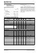
DC ELECTRICAL CHARACTERISTICS
Electrical Characteristics: Unless otherwise indicated, T
A
= +25°C
Parameters Sym Min Typ Max Units Conditions
Static Characteristics
Drain-to-Source
Breakdown Voltage
B
VDSS
25 — — V V
GS
= 0V, I
D
= 250 µA
Drain-to-Source Leakage Current I
DSS
—— 1µAV
GS
= 0V, V
DS
= 20V
Gate-to-Source Leakage Current I
GSS
——100nAV
DS
= 0V, V
GS
= 10V/-8V
Gate-to-Source Threshold Voltage V
GS(TH)
1.1 1.35 1.7 V V
DS
= V
GS
, I
D
= 250 µA
Drain-to-Source On Resistance R
DS(ON)
— 17.3 — m V
GS
= 3.3V, I
D
= 10A
— 13.8 16.5 m
V
GS
= 4.5V, I
D
= 10A
—11.313.5m
V
GS
= 10V, I
D
= 10A
Transconductance g
fs
—40— SV
DS
= 12.5V, I
D
= 10A
Dynamic Characteristics
Input Capacitance C
ISS
—400— pFV
GS
= 0V, V
DS
= 12.5V, f = 1 MHz
Output Capacitance C
OSS
—200— pFV
GS
= 0V, V
DS
= 12.5V, f = 1 MHz
Reverse Transfer Capacitance C
RSS
—60—pFV
GS
= 0V, V
DS
= 12.5V, f = 1 MHz
Total Gate Charge Q
G
—5.5 8 nCV
DS
= 12.5V, I
D
= 10A, V
GS
= 4.5V
Gate-to-Drain Charge Q
GD
—2.6—nCV
DS
= 12.5V, I
D
= 10A
Gate-to-Source Charge Q
GS
—0.9—nCV
DS
= 12.5V, I
D
= 10A
Gate Charge at V
GS(TH)
Q
G(TH)
—0.6—nCV
DS
= 12.5V, I
D
= 10A
Output Charge Q
OSS
—3.7—nCV
DS
= 12.5V, V
GS
= 0
Turn-On Delay Time t
d(on)
—2.2— nsV
DS
= 12.5V, V
GS
= 4.5V,
I
D
= 10A, R
G
= 2
Rise Time t
r
—5.4— nsV
DS
= 12.5V, V
GS
= 4.5V,
I
D
= 10A, R
G
= 2
Turn-Off Delay Time t
d(off)
—4.2— nsV
DS
= 12.5V, V
GS
= 4.5V,
I
D
= 10A, R
G
= 2
Fall Time t
f
—2.1— nsV
DS
= 12.5V, V
GS
= 4.5V,
I
D
= 10A, R
G
= 2
Series Gate Resistance R
G
—1.7—