
User's Manual
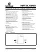
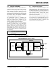
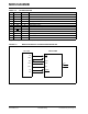
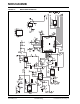
Table Of Contents
- Features:
- Operational:
- RF/Analog Features:
- MAC/Baseband Features:
- Table of Contents
- Most Current Data Sheet
- Errata
- Customer Notification System
- 1.0 Device Overview
- 2.0 Circuit Description
- 3.0 Regulatory Approval
- 4.0 Electrical Characteristics
- Appendix A: Revision History
- INDEX
- The Microchip Web Site
- Customer Change Notification Service
- Customer Support
- Reader Response
- Product Identification System

MRF24J40MB
DS70599B-page 4 Preliminary © 2009 Microchip Technology Inc.
FIGURE 1-2: MICROCONTROLLER TO MRF24J40MB INTERFACE
TABLE 1-1: PIN DESCRIPTION
Pin Symbol Type Description
1 GND Power Ground
2 RESET DI Global hardware Reset pin
3 WAKE DI External wake-up trigger
4 INT DO Interrupt pin to microcontroller
5 SDI DI Serial interface data input
6 SCK DI Serial interface clock
7 SDO DO Serial interface data output from MRF24J40
8CS
DI Serial interface enable
9 NC — No connection
10 VIN Power Power supply
11 GND Ground Ground
12 GND Ground Ground
Legend: Pin type abbreviation: D = Digital, I = Input, O = Output
SDO
I/O
SDI
SCK
INTx
MRF24J40MB
CS
SDI
SDO
SCK
INT
I/O
WAKE
VIN
GND
PIC
®
MCU
I/O
RESET