
User's Manual


ATSAMR30M18A User manual
1. RF Trace Layout Design Instructions for host ATSAMR30M Sensor Board
The ATSAMR30M18A module transmitter is certified with
• On-board PCB antenna and micro strip layout
This section describes the PCB stack up, mechanical details of the PCB trace leading up to PCB antenna.
The host PCB can follow these trace design to maintain compliance under the modular grant (FCC) and
Canada certificate (IC). Schematics, BoM, Layout source files and Gerber files are available for customer
use.
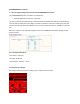
Below is a snapshot of the schematic diagram for the host ATSAMR30 Sensor Board showing the PCB
Antenna section.
2.1 Trace layout dimensions:
Trace width – 0.533 mm
Trace gap – 0.381 mm
Finished copper thickness – 47um
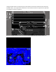
2.2 Layout of Trace design:
Below figure shows the Top layer routing of the complete reference board.