
Datasheet


2010 Microchip Technology Inc. DS21754M-page 3
24AA512/24LC512/24FC512
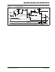
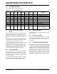
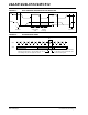
TABLE 1-2: AC CHARACTERISTICS
AC CHARACTERISTICS
Electrical Characteristics:
Industrial (I): V
CC = +1.7V to 5.5V TA = -40°C to +85°C
Automotive (E): V
CC = +2.5V to 5.5V TA = -40°C to +125°C
Param.
No.
Sym. Characteristic Min. Max. Units Conditions
1
FCLK Clock frequency —
—
—
—
100
400
400
1000
kHz 1.7V VCC 2.5V
2.5V V
CC 5.5V
1.7V V
CC 2.5V 24FC512
2.5V V
CC 5.5V 24FC512
2
THIGH Clock high time 4000
600
600
500
—
—
—
—
ns 1.7V VCC 2.5V
2.5V V
CC 5.5V
1.7V V
CC 2.5V 24FC512
2.5V V
CC 5.5V 24FC512
3
TLOW Clock low time 4700
1300
1300
500
—
—
—
—
ns 1.7V VCC 2.5V
2.5V V
CC 5.5V
1.7V V
CC 2.5V 24FC512
2.5V V
CC 5.5V 24FC512
4
TR SDA and SCL rise time (Note 1) —
—
—
1000
300
300
ns 1.7V VCC< 2.5V
2.5V V
CC 5.5V
1.7V V
CC 5.5V 24FC512
5
TF SDA and SCL fall time (Note 1) —
—
300
100
ns All except, 24FC512
1.7V V
CC 5.5V 24FC512
6
THD:STA Start condition hold time 4000
600
600
250
—
—
—
—
ns 1.7V VCC 2.5V
2.5V V
CC 5.5V
1.7V V
CC 2.5V 24FC512
2.5V V
CC 5.5V 24FC512
7
TSU:STA Start condition setup time 4700
600
600
250
—
—
—
—
ns 1.7V VCC 2.5V
2.5V V
CC 5.5V
1.7V V
CC 2.5V 24FC512
2.5V V
CC 5.5V 24FC512
8
THD:DAT Data input hold time 0 — ns (Note 2)
9
TSU:DAT Data input setup time 250
100
100
—
—
—
ns 1.7V VCC 2.5V
2.5V V
CC 5.5V
1.7V V
CC 5.5V 24FC512
10
TSU:STO Stop condition setup time 4000
600
600
250
—
—
—
—
ns 1.7V VCC 2.5V
2.5V V
CC 5.5V
1.7V V
CC 2.5V 24FC512
2.5V V
CC 5.5V 24FC512
11
TSU:WP WP setup time 4000
600
600
—
—
—
ns 1.7V VCC 2.5V
2.5V V
CC 5.5V
1.7V V
CC 5.5V 24FC512
12
THD:WP WP hold time 4700
1300
1300
—
—
—
ns 1.7V VCC 2.5V
2.5V V
CC 5.5V
1.7V V
CC 5.5V 24FC512
13
TAA Output valid from clock (Note 2) —
—
—
—
3500
900
900
400
ns 1.7V VCC 2.5V
2.5V V
CC 5.5V
1.7V V
CC 2.5V 24FC512
2.5V V
CC 5.5V 24FC512
14
TBUF Bus free time: Time the bus
must be free before a new trans-
mission can start
4700
1300
1300
500
—
—
—
—
ns 1.7V VCC 2.5V
2.5V V
CC 5.5V
1.7V V
CC 2.5V 24FC512
2.5V V
CC 5.5V 24FC512
Note 1: Not 100% tested. C
B = total capacitance of one bus line in pF.
2: As a transmitter, the device must provide an internal minimum delay time to bridge the undefined region (minimum
300 ns) of the falling edge of SCL to avoid unintended generation of Start or Stop conditions.
3: The combined T
SP and VHYS specifications are due to new Schmitt Trigger inputs which provide improved noise spike
suppression. This eliminates the need for a T
I specification for standard operation.
4: This parameter is not tested but ensured by characterization. For endurance estimates in a specific application, please
consult the Total Endurance™ Model which can be obtained from Microchip’s web site at www.microchip.com.