
Datasheet
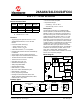

1997-2012 Microchip Technology Inc. DS21189T-page 1
24AA64/24LC64/24FC64
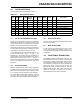
Device Selection Table
Features:
• Single-Supply with Operation down to 1.7V for
24AA64/24FC64 Devices, 2.5V for 24LC64
Devices
• Low-Power CMOS Technology:
- Active current 3 mA, max.
- Standby current 1 A, max.
• 2-Wire Serial Interface, I
2
C™ Compatible
• Packages with 3 Address Pins are Cascadable up
to 8 Devices
• Schmitt Trigger Inputs for Noise Suppression
• Output Slope Control to Eliminate Ground Bounce
• 100 kHz and 400 kHz Clock Compatibility
• 1 MHz Clock for FC versions
• Page Write Time 5 ms, max.
• Self-timed Erase/Write Cycle
• 32-Byte Page Write Buffer
• Hardware Write-Protect
• ESD Protection > 4,000V
• More than 1 Million Erase/Write Cycles
• Data Retention > 200 Years
• Factory Programming Available
• Packages include 8-lead PDIP, SOIC, SOIJ,
TSSOP, X-Rotated TSSOP, MSOP, DFN, TDFN,
5-lead SOT-23 or Chip Scale
• Pb-Free and RoHS Compliant
• Temperature Ranges:
- Industrial (I): -40°C to +85°C
- Automotive (E): -40°C to +125°C
Description:
The Microchip Technology Inc. 24AA64/24LC64/
24FC64 (24XX64*) is a 64 Kbit Electrically Erasable
PROM. The device is organized as a single block of
8K x 8-bit memory with a 2-wire serial interface. Low-
voltage design permits operation down to 1.7V, with
standby and active currents of only 1 A and 3 mA,
respectively. It has been developed for advanced, low-
power applications such as personal communications
or data acquisition. The 24XX64 also has a page write
capability for up to 32 bytes of data. Functional
address lines allow up to eight devices on the same
bus, for up to 512 Kbits address space. The 24XX64 is
available in the standard 8-pin PDIP, surface mount
SOIC, SOIJ, TSSOP, DFN, TDFN and MSOP
packages. The 24XX64 is also available in the 5-lead
SOT-23, and Chip Scale packages.
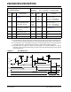
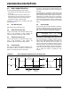
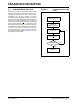
Block Diagram
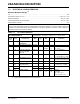
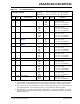
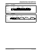
Package Types
Part
Number
VCC
Range
Max. Clock
Frequency
Temp.
Ranges
24AA64 1.7-5.5 400 kHz
(1)
I, E
24LC64 2.5-5.5 400 kHz I, E
24FC64 1.7-5.5 1 MHz
(2)
I
Note 1: 100 kHz for V
CC <2.5V.
2: 400 kHz for V
CC <2.5V.
HV
EEPROM
Array
Page
YDEC
XDEC
Sense Amp.
Memory
Control
Logic
I/O
Control
Logic
I/O
WP
SDA
SCL
V
CC
VSS
R/W Control
Latches
Generator
A2A1A0
A0
A1
A2
V
SS
V
CC
WP
SCL
SDA
1
2
3
4
8
7
6
5
PDIP/MSOP/SOIC/SOIJ/TSSOP
DFN/TDFN
A0
A1
A2
V
SS
WP
SCL
SDA
V
CC
8
7
6
5
1
2
3
4
SOT-23
1
2
34
5
WP
V
CC
SCL
V
SS
SDA
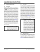
CS (Chip Scale)
(1)
1
2
3
45
V
CC
WP
SDA
SCL
V
SS
(Top Down View,
Balls Not Visible)
Note 1: Available in I-temp, “AA” only.
X-Rotated TSSOP
WP
V
CC
A0
A1
1
2
3
4
8
7
6
5
SCL
SDA
V
SS
A2
(X/ST)
64K I
2
C™ Serial EEPROM
* 24XX64 is used in this document as a generic part number for the 24AA64/24LC64/24FC64 devices.