
User Guide
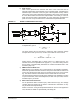
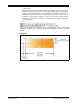
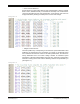
Table Of Contents
- 1.1 SETTING SOFTWARE PARAMETERS
- Corporate Office
- Atlanta
- Boston
- Chicago
- Cleveland
- Fax: 216-447-0643
- Dallas
- Detroit
- Kokomo
- Toronto
- Fax: 852-2401-3431
- Australia - Sydney
- China - Beijing
- China - Shanghai
- India - Bangalore
- Korea - Daegu
- Korea - Seoul
- Singapore
- Taiwan - Taipei
- Fax: 43-7242-2244-393
- Denmark - Copenhagen
- France - Paris
- Germany - Munich
- Italy - Milan
- Spain - Madrid
- UK - Wokingham
- Worldwide Sales and Service

DS70640A-page 2 2010 Microchip Technology Inc.
b) Peak Current
Peak current represents the maximum real value of the current that can be
internally represented, which depends on the acquisition block. Considering the
maximum input to the ADC of 3.3V, the gain of the acquisition circuitry and the
value of the current shunts determine the maximum value of the current that will
fit to the dsPIC
®
DSC internal number representation. Conversely, a current of
which the internal number representation is at the upper limit, represents the
peak current as it may be entered in the indicated Excel spreadsheet field.
FIGURE 1-2: SIGNAL CONDITIONING CIRCUITRY
For the circuit presented in Figure 1-2 above, the current acquisition circuitry has
an amplification gain of:
The shunt resistor value for the MCLV is 5 mΩ and, with a maximum voltage
accepted at the ADC input of 3.3V, results in the maximum current read of:
Notice that the calculated value of Peak current (I
max
) differs from the one
indicated in the Excel spreadsheet file (Figure 1-1) – the reason being that the
second value is experimentally determined as it will be described later in this
document (Step 3-d).
c) PWM Period and Dead Time
PWM Period is the sampling and control period for this algorithm (AN1292).
Dead time represents the time needed for the power semiconductor devices to
recover from the previous state so that no shoot-through occurs on any inverter
leg. The values entered in these fields should coincide with the ones used.
The demonstration software included in the application note implements a value
of 2 µs for dead time, and for the PWM period, a value of 50 µs is used, which is
a PWM frequency of 20 kHz.
d) Motor’s Electrical Parameters
For the parameters Stator resistance (Rs), Stator inductance (Ls), and Voltage
constant (Kfi) enter them from the motor’s manufacturer’s information or they
may be determined experimentally.
Please consult the “Tuning and Experimental Results” section of the application
note, AN1292 for details on experimentally calculating Kfi.
1
2
3
A
m
Single Shunt
G
R20
R22 R23+
--------------------------
75==
I
max
V
REF
Shunt Gain
--------------------------------
3.3
2
-------
0.005 75
------------------------
4.4A===