
Datasheet

2016 Microchip Technology Inc. DS00002164B-page 63
LAN8710A/LAN8710AI
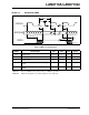
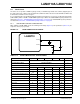
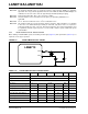
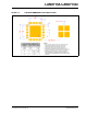
5.5.5 RMII INTERFACE TIMING
FIGURE 5-6: RMII TIMING
CLKIN
(REF_CLK)
RXD[1:0],
RXER
CRS_DV
t
clkh
t
clkl
t
clkp
t
oval
t
ohold
t
oval
t
oval
t
ohold
t
su
TXD[1:0]
TXEN
t
ihold
t
su
t
ihold
t
ihold
t
su
t
ihold
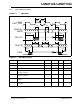
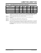
TABLE 5-9: RMII TIMING VALUES
Symbol Description Min Max Units Notes
t
clkp
CLKIN period 20 — ns —
t
clkh
CLKIN high time t
clkp
*0.35 t
clkp
*0.65 ns —
t
clkl
CLKIN low time t
clkp
*0.35 t
clkp
*0.65 ns —
t
oval
RXD[1:0], RXER, CRS_DV output valid from ris-
ing edge of CLKIN
— 14.0 ns Note 5-25
t
ohold
RXD[1:0], RXER, CRS_DV output hold from ris-
ing edge of CLKIN
3.0 — ns Note 5-25
t
su
TXD[1:0], TXEN setup time to rising edge of
CLKIN
4.0 — ns Note 5-25
t
ihold
TXD[1:0], TXEN input hold time after rising edge
of CLKIN
1.5 — ns Note 5-25
Note 5-25 T
iming was designed for system load between 10 pf and 25 pf.