
Datasheet


© 2011 Microchip Technology Inc. DS25005A-page 3
MCP14E9/10/11
1.0 ELECTRICAL
CHARACTERISTICS
Absolute Maximum Ratings †
Supply Voltage ................................................................+20V
Input Voltage ...............................(V
DD
+ 0.3V) to (GND – 5V)
Enable Voltage............................(V
DD
+ 0.3V) to (GND – 5V)
Input Current (V
IN
>V
DD
)................................................50 mA
Package Power Dissipation (T
A
= +50
o
C)
8L-DFN ........................................................................Note 3
8L-PDIP ........................................................................1.12W
8L-SOIC .....................................................................669 mW
† Notice: Stresses above those listed under “Maximum
Ratings” may cause permanent damage to the device.
This is a stress rating only and functional operation of
the device at those or any other conditions above those
indicated in the operational sections of this specifica-
tion is not intended. Exposure to maximum rating
conditions for extended periods may affect device
reliability.
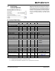
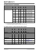
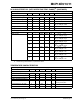
DC CHARACTERISTICS
(2)
Electrical Specifications: Unless otherwise indicated, T
A
= +25°C, with 4.5V ≤ V
DD
≤ 18V.
Parameters Sym Min Typ Max Units Conditions
Input
Logic ‘1’, High Input Voltage V
IH
2.4 1.5 — V
Logic ‘0’, Low Input Voltage V
IL
—1.30.8V
Input Current I
IN
-1 — 1 µA 0V ≤ V
IN
≤ V
DD
Input Voltage V
IN
-5 — V
DD
+ 0.3 V
Output
High Output Voltage V
OH
V
DD
– 0.025 — — V DC Test
Low Output Voltage V
OL
— — 0.025 V DC Test
Output Resistance, High R
OH
—47Ω I
OUT
= 10 mA, V
DD
= 18V
Output Resistance, Low R
OL
—47Ω I
OUT
= 10 mA, V
DD
= 18V
Peak Output Current I
PK
—3—AV
DD
= 18V
(2)
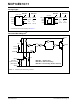
Switching Time
(1)
Rise Time t
R
—1430nsFigure 4-1, Figure 4-2,
C
L
= 1800 pF
Fall Time t
F
—1730nsFigure 4-1, Figure 4-2,
C
L
= 1800 pF
Propagation Delay Time t
D1
—4555nsFigure 4-1, Figure 4-2
Propagation Delay Time t
D2
—4555nsFigure 4-1, Figure 4-2
Enable Function (ENB_A, ENB_B)
High-Level Input Voltage V
EN_H
2.4 1.6 — V V
DD
= 12V, Low-to-High Transition
Low-Level Input Voltage V
EN_L
—1.20.8VV
DD
= 12V, High-to-Low Transition
Hysteresis V
HYST
—400—mV
Enable Pull-up Impedance R
ENBL
0.7 1.6 3.0 MΩ V
DD
= 14V, ENBL = GND
Enable Pin Leakage Current I
ENBL
—10—µAV
DD
=12V,
ENB_A = ENB_B = GND
Propagation Delay Time t
D3
—3565nsV
DD
=12V, Figure 4-3
Propagation Delay Time t
D4
—3565nsV
DD
=12V, Figure 4-3
Note 1: Switching times are ensured by design.
2: Tested during characterization, not production tested.
3: Package power dissipation is dependent on the copper pad area of the PCB.