
Datasheet


MCP1700
DS21826B-page 4 © 2007 Microchip Technology Inc.
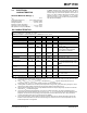
TEMPERATURE SPECIFICATIONS
Power Supply Ripple
Rejection Ratio
PSRR — 44 — dB f = 100 Hz, C
OUT
=1µF, I
L
=50mA,
V
INAC
=100mVpk-pk, C
IN
=0µF,
V
R
=1.2V
Thermal Shutdown Protection T
SD
— 140 — °C V
IN
=V
R
+1, I
L
= 100 µA
Electrical Characteristics: Unless otherwise specified, all limits are established for V
IN
=V
R
+1, I
LOAD
= 100 µA,
C
OUT
= 1 µF (X7R), C
IN
=1µF (X7R), T
A
= +25°C.
Boldface type applies for junction temperatures, T
J
(Note 1) of -40°C to +125°C.
Parameters Sym Min Typ Max Units Conditions
Temperature Ranges
Specified Temperature Range T
A
-40 +125 °C
Operating Temperature Range T
A
-40 +125 °C
Storage Temperature Range T
A
-65 +150 °C
Thermal Package Resistance
Thermal Resistance, SOT-23
θ
JA
—336—°C/W
Minimum Trace Width Single Layer
Board
— 230 — °C/W Typical FR4 4-layer Application
Thermal Resistance, SOT-89 θ
JA
— 52 — °C/W Typical, 1 square inch of copper
Thermal Resistance, TO-92
θ
JA
— 131.9 — °C/W
EIA/JEDEC JESD51-751-7
4-Layer Board
Note 1: The maximum allowable power dissipation is a function of ambient temperature, the maximum allowable junction
temperature and the thermal resistance from junction to air (i.e., T
A
, T
J
, θ
JA
). Exceeding the maximum allowable power
dissipation will cause the device operating junction temperature to exceed the maximum 150°C rating. Sustained
junction temperatures above 150°C can impact the device reliability.
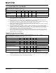
DC CHARACTERISTICS (CONTINUED)
Electrical Characteristics: Unless otherwise specified, all limits are established for V
IN
=V
R
+1, I
LOAD
= 100 µA,
C
OUT
=1µF (X7R), C
IN
=1µF(X7R), T
A
= +25°C.
Boldface type applies for junction temperatures, T
J
(Note 6) of -40°C to +125°C.
Parameters Sym Min Typ Max Units Conditions
Note 1: The minimum V
IN
must meet two conditions: V
IN
≥ 2.3V and V
IN
≥ (V
R
+ 3.0%) +V
DROPOUT
.
2: V
R
is the nominal regulator output voltage. For example: V
R
= 1.2V, 1.5V, 1.8V, 2.5V, 2.8V, 3.0V, 3.3V, 4.0V, 5.0V. The
input voltage (V
IN
=V
R
+ 1.0V); I
OUT
= 100 µA.
3: TCV
OUT
= (V
OUT-HIGH
-V
OUT-LOW
) *10
6
/ (V
R
* ΔTemperature), V
OUT-HIGH
= highest voltage measured over the
temperature range. V
OUT-LOW
= lowest voltage measured over the temperature range.
4: Load regulation is measured at a constant junction temperature using low duty cycle pulse testing. Changes in output
voltage due to heating effects are determined using thermal regulation specification TCV
OUT
.
5: Dropout voltage is defined as the input to output differential at which the output voltage drops 2% below its measured
value with a V
R
+ 1V differential applied.
6: The maximum allowable power dissipation is a function of ambient temperature, the maximum allowable junction
temperature and the thermal resistance from junction to air (i.e., T
A
, T
J
, θ
JA
). Exceeding the maximum allowable power
dissipation will cause the device operating junction temperature to exceed the maximum 150°C rating. Sustained
junction temperatures above 150°C can impact the device reliability.
7: The junction temperature is approximated by soaking the device under test at an ambient temperature equal to the
desired Junction temperature. The test time is small enough such that the rise in the Junction temperature over the
ambient temperature is not significant.